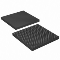
EP1S10F672C7 Altera, EP1S10F672C7 Datasheet - Page 105

EP1S10F672C7
Manufacturer Part Number
EP1S10F672C7
Description
IC STRATIX FPGA 10K LE 672-FBGA
Manufacturer
Altera
Series
Stratix®r
Datasheet
1.EP1S10F780C7.pdf
(276 pages)
Specifications of EP1S10F672C7
Number Of Logic Elements/cells
10570
Number Of Labs/clbs
1057
Total Ram Bits
920448
Number Of I /o
345
Voltage - Supply
1.425 V ~ 1.575 V
Mounting Type
Surface Mount
Operating Temperature
0°C ~ 85°C
Package / Case
672-FBGA
Family Name
Stratix
Number Of Logic Blocks/elements
10570
# I/os (max)
345
Frequency (max)
420.17MHz
Process Technology
0.13um (CMOS)
Operating Supply Voltage (typ)
1.5V
Logic Cells
10570
Ram Bits
920448
Operating Supply Voltage (min)
1.425V
Operating Supply Voltage (max)
1.575V
Operating Temp Range
0C to 85C
Operating Temperature Classification
Commercial
Mounting
Surface Mount
Pin Count
672
Package Type
FBGA
Lead Free Status / RoHS Status
Contains lead / RoHS non-compliant
Number Of Gates
-
Lead Free Status / Rohs Status
Not Compliant
Other names
544-1109
Available stocks
Company
Part Number
Manufacturer
Quantity
Price
Company:
Part Number:
EP1S10F672C7
Manufacturer:
ALTERA
Quantity:
3 000
Part Number:
EP1S10F672C7
Manufacturer:
XILINX/赛灵思
Quantity:
20 000
Company:
Part Number:
EP1S10F672C7AA
Manufacturer:
ALTERA
Quantity:
3 000
Company:
Part Number:
EP1S10F672C7ES
Manufacturer:
ALTERA
Quantity:
89
Company:
Part Number:
EP1S10F672C7N
Manufacturer:
ALTERA
Quantity:
3 000
Part Number:
EP1S10F672C7N
Manufacturer:
ALTERA/阿尔特拉
Quantity:
20 000
Figure 2–54. Dynamically Programmable Counters & Delays in Stratix Device Enhanced PLLs
Altera Corporation
July 2005
scandata
scanaclr
scanclk
f
REF
÷n
Counters and Clock
Delay Settings are
Programmable
f
Δt
PLL reconfiguration data is shifted into serial registers from the logic
array or external devices. The PLL input shift data uses a reference input
shift clock. Once the last bit of the serial chain is clocked in, the register
chain is synchronously loaded into the PLL configuration bits. The shift
circuitry also provides an asynchronous clear for the serial registers.
For more information on PLL reconfiguration, see AN 282: Implementing
PLL Reconfiguration in Stratix & Stratix GX Devices.
Programmable Bandwidth
You have advanced control of the PLL bandwidth using the
programmable control of the PLL loop characteristics, including loop
filter and charge pump. The PLL’s bandwidth is a measure of its ability to
track the input clock and jitter. A high-bandwidth PLL can quickly lock
onto a reference clock and react to any changes in the clock. It also will
allow a wide band of input jitter spectrum to pass to the output. A low-
bandwidth PLL will take longer to lock, but it will attenuate all high-
frequency jitter components. The Quartus II software can adjust PLL
characteristics to achieve the desired bandwidth. The programmable
PFD
÷m
Charge
Pump
Δt
Loop
Filter
VCO
Stratix Device Handbook, Volume 1
All Output Counters and
Clock Delay Settings can
be Programmed Dynamically
÷g
÷e
÷l
Stratix Architecture
Δt
Δt
Δt
2–91


