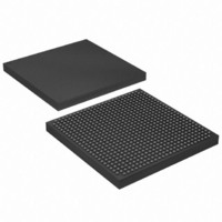
EP1S10F672C7 Altera, EP1S10F672C7 Datasheet - Page 52

EP1S10F672C7
Manufacturer Part Number
EP1S10F672C7
Description
IC STRATIX FPGA 10K LE 672-FBGA
Manufacturer
Altera
Series
Stratix®r
Datasheet
1.EP1S10F780C7.pdf
(276 pages)
Specifications of EP1S10F672C7
Number Of Logic Elements/cells
10570
Number Of Labs/clbs
1057
Total Ram Bits
920448
Number Of I /o
345
Voltage - Supply
1.425 V ~ 1.575 V
Mounting Type
Surface Mount
Operating Temperature
0°C ~ 85°C
Package / Case
672-FBGA
Family Name
Stratix
Number Of Logic Blocks/elements
10570
# I/os (max)
345
Frequency (max)
420.17MHz
Process Technology
0.13um (CMOS)
Operating Supply Voltage (typ)
1.5V
Logic Cells
10570
Ram Bits
920448
Operating Supply Voltage (min)
1.425V
Operating Supply Voltage (max)
1.575V
Operating Temp Range
0C to 85C
Operating Temperature Classification
Commercial
Mounting
Surface Mount
Pin Count
672
Package Type
FBGA
Lead Free Status / RoHS Status
Contains lead / RoHS non-compliant
Number Of Gates
-
Lead Free Status / Rohs Status
Not Compliant
Other names
544-1109
Available stocks
Company
Part Number
Manufacturer
Quantity
Price
Company:
Part Number:
EP1S10F672C7
Manufacturer:
ALTERA
Quantity:
3 000
Part Number:
EP1S10F672C7
Manufacturer:
XILINX/赛灵思
Quantity:
20 000
Company:
Part Number:
EP1S10F672C7AA
Manufacturer:
ALTERA
Quantity:
3 000
Company:
Part Number:
EP1S10F672C7ES
Manufacturer:
ALTERA
Quantity:
89
Company:
Part Number:
EP1S10F672C7N
Manufacturer:
ALTERA
Quantity:
3 000
Part Number:
EP1S10F672C7N
Manufacturer:
ALTERA/阿尔特拉
Quantity:
20 000
TriMatrix Memory
Figure 2–20. EP1S60 Device with M-RAM Interface Locations
Note to
(1)
2–38
Stratix Device Handbook, Volume 1
Device shown is an EP1S60 device. The number and position of M-RAM blocks varies in other devices.
Figure
Blocks
DSP
2–20:
Blocks
top, bottom, and side opposite
M512
M-RAM
M-RAM
M-RAM pairs interface to
of block-to-block border.
Block
Block
The M-RAM block local interconnect is driven by the R4, R8, C4, C8, and
direct link interconnects from adjacent LABs. For independent M-RAM
blocks, up to 10 direct link address and control signal input connections
to the M-RAM block are possible from the left adjacent LABs for M-RAM
M-RAM
M-RAM
Block
Block
Blocks
M4K
Note (1)
LABs
interface to top, bottom, and side facing
device perimeter for easy access
M-RAM
M-RAM
Independent M-RAM blocks
Block
Block
to horizontal I/O pins.
Altera Corporation
Blocks
DSP
July 2005


