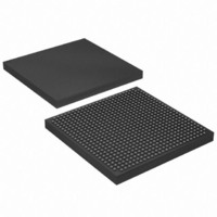
EP1S10F672C7 Altera, EP1S10F672C7 Datasheet - Page 50

EP1S10F672C7
Manufacturer Part Number
EP1S10F672C7
Description
IC STRATIX FPGA 10K LE 672-FBGA
Manufacturer
Altera
Series
Stratix®r
Datasheet
1.EP1S10F780C7.pdf
(276 pages)
Specifications of EP1S10F672C7
Number Of Logic Elements/cells
10570
Number Of Labs/clbs
1057
Total Ram Bits
920448
Number Of I /o
345
Voltage - Supply
1.425 V ~ 1.575 V
Mounting Type
Surface Mount
Operating Temperature
0°C ~ 85°C
Package / Case
672-FBGA
Family Name
Stratix
Number Of Logic Blocks/elements
10570
# I/os (max)
345
Frequency (max)
420.17MHz
Process Technology
0.13um (CMOS)
Operating Supply Voltage (typ)
1.5V
Logic Cells
10570
Ram Bits
920448
Operating Supply Voltage (min)
1.425V
Operating Supply Voltage (max)
1.575V
Operating Temp Range
0C to 85C
Operating Temperature Classification
Commercial
Mounting
Surface Mount
Pin Count
672
Package Type
FBGA
Lead Free Status / RoHS Status
Contains lead / RoHS non-compliant
Number Of Gates
-
Lead Free Status / Rohs Status
Not Compliant
Other names
544-1109
Available stocks
Company
Part Number
Manufacturer
Quantity
Price
Company:
Part Number:
EP1S10F672C7
Manufacturer:
ALTERA
Quantity:
3 000
Part Number:
EP1S10F672C7
Manufacturer:
XILINX/赛灵思
Quantity:
20 000
Company:
Part Number:
EP1S10F672C7AA
Manufacturer:
ALTERA
Quantity:
3 000
Company:
Part Number:
EP1S10F672C7ES
Manufacturer:
ALTERA
Quantity:
89
Company:
Part Number:
EP1S10F672C7N
Manufacturer:
ALTERA
Quantity:
3 000
Part Number:
EP1S10F672C7N
Manufacturer:
ALTERA/阿尔特拉
Quantity:
20 000
TriMatrix Memory
2–36
Stratix Device Handbook, Volume 1
Similar to all RAM blocks, M-RAM blocks can have different clocks on
their inputs and outputs. All input registers—renwe, datain, address,
and byte enable registers—are clocked together from either of the two
clocks feeding the block. The output register can be bypassed. The eight
labclk signals or local interconnect can drive the control signals for the
A and B ports of the M-RAM block. LEs can also control the clock_a,
clock_b, renwe_a, renwe_b, clr_a, clr_b, clocken_a, and
clocken_b signals as shown in
Notes to
(1)
(2)
Table 2–11. M-RAM Combined Byte Selection for ×144 Mode
Any combination of byte enables is possible.
Byte enables can be used in the same manner with 8-bit words, i.e., in × 16, × 32,
× 64, and × 128 modes.
Tables 2–10
byteena[15..0]
[10] = 1
[11] = 1
[12] = 1
[13] = 1
[14] = 1
[15] = 1
[0] = 1
[1] = 1
[2] = 1
[3] = 1
[4] = 1
[5] = 1
[6] = 1
[7] = 1
[8] = 1
[9] = 1
and 2–11:
Figure
2–19.
datain ×144
[116..108]
[125..117]
[134..126]
[143..135]
[107..99]
[26..18]
[35..27]
[44..36]
[53..45]
[62..54]
[71..63]
[80..72]
[89..81]
[98..90]
[17..9]
[8..0]
Altera Corporation
Notes
July 2005
(1),
(2)


