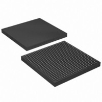
EP1S10F672C7 Altera, EP1S10F672C7 Datasheet - Page 206

EP1S10F672C7
Manufacturer Part Number
EP1S10F672C7
Description
IC STRATIX FPGA 10K LE 672-FBGA
Manufacturer
Altera
Series
Stratix®r
Datasheet
1.EP1S10F780C7.pdf
(276 pages)
Specifications of EP1S10F672C7
Number Of Logic Elements/cells
10570
Number Of Labs/clbs
1057
Total Ram Bits
920448
Number Of I /o
345
Voltage - Supply
1.425 V ~ 1.575 V
Mounting Type
Surface Mount
Operating Temperature
0°C ~ 85°C
Package / Case
672-FBGA
Family Name
Stratix
Number Of Logic Blocks/elements
10570
# I/os (max)
345
Frequency (max)
420.17MHz
Process Technology
0.13um (CMOS)
Operating Supply Voltage (typ)
1.5V
Logic Cells
10570
Ram Bits
920448
Operating Supply Voltage (min)
1.425V
Operating Supply Voltage (max)
1.575V
Operating Temp Range
0C to 85C
Operating Temperature Classification
Commercial
Mounting
Surface Mount
Pin Count
672
Package Type
FBGA
Lead Free Status / RoHS Status
Contains lead / RoHS non-compliant
Number Of Gates
-
Lead Free Status / Rohs Status
Not Compliant
Other names
544-1109
Available stocks
Company
Part Number
Manufacturer
Quantity
Price
Company:
Part Number:
EP1S10F672C7
Manufacturer:
ALTERA
Quantity:
3 000
Part Number:
EP1S10F672C7
Manufacturer:
XILINX/赛灵思
Quantity:
20 000
Company:
Part Number:
EP1S10F672C7AA
Manufacturer:
ALTERA
Quantity:
3 000
Company:
Part Number:
EP1S10F672C7ES
Manufacturer:
ALTERA
Quantity:
89
Company:
Part Number:
EP1S10F672C7N
Manufacturer:
ALTERA
Quantity:
3 000
Part Number:
EP1S10F672C7N
Manufacturer:
ALTERA/阿尔特拉
Quantity:
20 000
Timing Model
4–36
Stratix Device Handbook, Volume 1
t
t
t
t
t
t
t
t
t
t
t
t
t
t
t
INSU
INH
OUTCO
XZ
ZX
INSU
INH
OUTCO
XZ
ZX
INSUPLL
INHPLL
OUTCOPLL
XZPLL
ZXPLL
Table 4–55. EP1S10 External I/O Timing on Column Pins Using Fast Regional Clock Networks
Table 4–56. EP1S10 External I/O Timing on Column Pins Using Regional Clock Networks
Parameter
Parameter
1.992
0.000
2.395
2.335
2.335
0.975
0.000
1.262
1.202
1.202
2.238
0.000
2.240
2.180
2.180
-5 Speed Grade
-5 Speed Grade
Min
Min
4.795
4.669
4.669
2.636
2.510
2.510
4.549
4.423
4.423
Max
Max
Stratix External I/O Timing
These timing parameters are for both column IOE and row IOE pins. In
EP1S30 devices and above, you can decrease the t
FPLLCLK, but may get positive hold time in EP1S60 and EP1S80 devices.
You should use the Quartus II software to verify the external devices for
any pin.
Tables 4–55
and row pins for EP1S10 devices.
2.054
0.000
2.395
2.335
2.335
0.985
0.000
1.262
1.202
1.202
2.325
0.000
2.240
2.180
2.180
-6 Speed Grade
-6 Speed Grade
Min
Min
through
5.107
4.975
4.975
2.680
2.548
2.548
4.836
4.704
4.704
Max
Max
4–60
show the external timing parameters on column
2.359
0.000
2.395
2.335
2.335
1.097
0.000
1.262
1.202
1.202
2.668
0.000
2.240
2.180
2.180
-7 Speed Grade
-7 Speed Grade
Min
Min
5.527
5.403
5.403
2.769
2.645
2.645
5.218
5.094
5.094
Max
Max
-8 Speed Grade
-8 Speed Grade
Min
NA
NA
NA
NA
NA
NA
NA
NA
NA
NA
NA
NA
NA
NA
NA
SU
time by using the
Altera Corporation
Note (1)
Max
NA
NA
NA
NA
NA
NA
NA
NA
NA
NA
January 2006
Note (1)
Unit
Unit
ns
ns
ns
ns
ns
ns
ns
ns
ns
ns
ns
ns
ns
ns
ns


