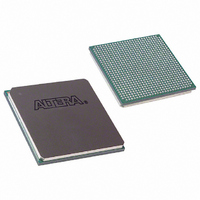
EP3C120F780C8N Altera, EP3C120F780C8N Datasheet - Page 104

EP3C120F780C8N
Manufacturer Part Number
EP3C120F780C8N
Description
IC CYCLONE III FPGA 119K 780FBGA
Manufacturer
Altera
Series
Cyclone® IIIr
Datasheets
1.EP3C5F256C8N.pdf
(5 pages)
2.EP3C5F256C8N.pdf
(34 pages)
3.EP3C5F256C8N.pdf
(66 pages)
4.EP3C5F256C8N.pdf
(14 pages)
5.EP3C5F256C8N.pdf
(76 pages)
6.EP3C120F780C8N.pdf
(274 pages)
Specifications of EP3C120F780C8N
Number Of Logic Elements/cells
119088
Number Of Labs/clbs
7443
Total Ram Bits
3981312
Number Of I /o
531
Voltage - Supply
1.15 V ~ 1.25 V
Mounting Type
Surface Mount
Operating Temperature
0°C ~ 85°C
Package / Case
780-FBGA
Family Name
Cyclone III
Number Of Logic Blocks/elements
119088
# I/os (max)
531
Frequency (max)
402MHz
Process Technology
65nm
Operating Supply Voltage (typ)
1.2V
Logic Cells
119088
Ram Bits
3981312
Operating Supply Voltage (min)
1.15V
Operating Supply Voltage (max)
1.25V
Operating Temp Range
0C to 85C
Operating Temperature Classification
Commercial
Mounting
Surface Mount
Pin Count
780
Package Type
FBGA
For Use With
544-2601 - KIT DEV CYCLONE III LS EP3CLS200544-2589 - KIT DEV EMB CYCLONE III EDITION544-2566 - KIT DEV DSP CYCLONE III EDITION544-2444 - KIT DEV CYCLONE III EP3C120544-2411 - KIT DEV NIOS II CYCLONE III ED.
Lead Free Status / RoHS Status
Lead free / RoHS Compliant
Number Of Gates
-
Lead Free Status / Rohs Status
Compliant
Other names
544-2392
544-2533
544-2533
EP3C120F780C8NES
544-2533
544-2533
EP3C120F780C8NES
Available stocks
Company
Part Number
Manufacturer
Quantity
Price
Company:
Part Number:
EP3C120F780C8N
Manufacturer:
ALTERA
Quantity:
642
Part Number:
EP3C120F780C8N
Manufacturer:
ALTERA/阿尔特拉
Quantity:
20 000
6–4
Slew Rate Control
Open-Drain Output
Bus Hold
Cyclone III Device Handbook, Volume 1
f
f
1
1
1
The output buffer for each Cyclone III device family I/O pin provides optional
programmable output slew-rate control. The Quartus II software allows three settings
for programmable slew rate control—0, 1, and 2—where 0 is the slow slew rate and 2
is the fast slew rate. The default setting is 2. A faster slew rate provides high-speed
transitions for high-performance systems. However, these fast transitions may
introduce noise transients in the system. A slower slew rate reduces system noise, but
adds a nominal delay to rising and falling edges. Because each I/O pin has an
individual slew-rate control, you can specify the slew rate on a pin-by-pin basis. The
slew-rate control affects both the rising and falling edges. Slew rate control is
available for single-ended I/O standards with current strength of 8 mA or higher.
You cannot use the programmable slew rate feature when using OCT with
calibration.
You cannot use the programmable slew rate feature when using the 3.0-V PCI,
3.0-V PCI-X, 3.3-V LVTTL, and 3.3-V LVCMOS I/O standards. Only fast slew rate
(default) setting is available.
For more information, refer to the
Quartus II Handbook.
The Cyclone III device family provides an optional open-drain (equivalent to an
open-collector) output for each I/O pin. This open-drain output enables the device to
provide system-level control signals (for example, interrupt and write enable signals)
that are asserted by multiple devices in your system.
For more information, refer to the
Quartus II Handbook.
Each Cyclone III device family user I/O pin provides an optional bus-hold feature.
The bus-hold circuitry holds the signal on an I/O pin at its last-driven state. Because
the bus-hold feature holds the last-driven state of the pin until the next input signal is
present, an external pull-up or pull-down resistor is not necessary to hold a signal
level when the bus is tri-stated.
The bus-hold circuitry also pulls undriven pins away from the input threshold
voltage in which noise can cause unintended high-frequency switching. You can
select this feature individually for each I/O pin. The bus-hold output drives no higher
than V
If you enable the bus-hold feature, the device cannot use the programmable pull-up
option. Disable the bus-hold feature when the I/O pin is configured for differential
signals. Bus-hold circuitry is not available on dedicated clock pins.
Bus-hold circuitry is only active after configuration. When going into user mode, the
bus-hold circuit captures the value on the pin present at the end of configuration.
CCIO
to prevent overdriving signals.
Assignment Editor
Assignment Editor
Chapter 6: I/O Features in the Cyclone III Device Family
chapter in volume 2 of the
chapter in volume 2 of the
© December 2009 Altera Corporation
I/O Element Features


