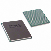
EP3C120F780C8N Altera, EP3C120F780C8N Datasheet - Page 47

EP3C120F780C8N
Manufacturer Part Number
EP3C120F780C8N
Description
IC CYCLONE III FPGA 119K 780FBGA
Manufacturer
Altera
Series
Cyclone® IIIr
Datasheets
1.EP3C5F256C8N.pdf
(5 pages)
2.EP3C5F256C8N.pdf
(34 pages)
3.EP3C5F256C8N.pdf
(66 pages)
4.EP3C5F256C8N.pdf
(14 pages)
5.EP3C5F256C8N.pdf
(76 pages)
6.EP3C120F780C8N.pdf
(274 pages)
Specifications of EP3C120F780C8N
Number Of Logic Elements/cells
119088
Number Of Labs/clbs
7443
Total Ram Bits
3981312
Number Of I /o
531
Voltage - Supply
1.15 V ~ 1.25 V
Mounting Type
Surface Mount
Operating Temperature
0°C ~ 85°C
Package / Case
780-FBGA
Family Name
Cyclone III
Number Of Logic Blocks/elements
119088
# I/os (max)
531
Frequency (max)
402MHz
Process Technology
65nm
Operating Supply Voltage (typ)
1.2V
Logic Cells
119088
Ram Bits
3981312
Operating Supply Voltage (min)
1.15V
Operating Supply Voltage (max)
1.25V
Operating Temp Range
0C to 85C
Operating Temperature Classification
Commercial
Mounting
Surface Mount
Pin Count
780
Package Type
FBGA
For Use With
544-2601 - KIT DEV CYCLONE III LS EP3CLS200544-2589 - KIT DEV EMB CYCLONE III EDITION544-2566 - KIT DEV DSP CYCLONE III EDITION544-2444 - KIT DEV CYCLONE III EP3C120544-2411 - KIT DEV NIOS II CYCLONE III ED.
Lead Free Status / RoHS Status
Lead free / RoHS Compliant
Number Of Gates
-
Lead Free Status / Rohs Status
Compliant
Other names
544-2392
544-2533
544-2533
EP3C120F780C8NES
544-2533
544-2533
EP3C120F780C8NES
Available stocks
Company
Part Number
Manufacturer
Quantity
Price
Company:
Part Number:
EP3C120F780C8N
Manufacturer:
ALTERA
Quantity:
642
Part Number:
EP3C120F780C8N
Manufacturer:
ALTERA/阿尔特拉
Quantity:
20 000
Chapter 3: Memory Blocks in the Cyclone III Device Family
Memory Modes
Figure 3–10. Cyclone III Device Family Simple Dual-Port Timing Waveforms
True Dual-Port Mode
© December 2009
q (asynch)
wraddress
rdaddress
wrclock
rdclock
wren
data
rden
1
Altera Corporation
din-1
doutn-1
an-1
Figure 3–10
dual-port mode with unregistered outputs. Registering the outputs of the RAM
simply delays the q output by one clock cycle.
True dual-port mode supports any combination of two-port operations: two reads,
two writes, or one read and one write, at two different clock frequencies.
shows the Cyclone III device family true dual-port memory configuration.
Figure 3–11. Cyclone III Device Family True Dual-Port Memory
Note to
(1) True dual-port memory supports input or output clock mode in addition to the independent clock mode shown.
The widest bit configuration of the M9K blocks in true dual-port mode is 512 × 16-bit
(18-bit with parity).
bn
Figure
an
din
3–11:
shows the timing waveforms for read and write operations in simple
doutn
b0
a0
a1
data_a[ ]
address_a[ ]
wren_a
byteena_a[]
addressstall_a
clocken_a
rden_a
aclr_a
q_a[]
clock_a
dout0
a2
b1
a3
addressstall_b
address_b[]
byteena_b[]
clocken_b
data_b[ ]
clock_b
wren_b
rden_b
aclr_b
q_b[]
din4
b2
a4
(Note 1)
Cyclone III Device Handbook, Volume 1
din5
a5
b3
a6
din6
Figure 3–11
3–11


