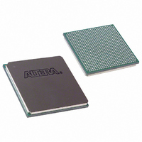
EP3C120F780C8N Altera, EP3C120F780C8N Datasheet - Page 211

EP3C120F780C8N
Manufacturer Part Number
EP3C120F780C8N
Description
IC CYCLONE III FPGA 119K 780FBGA
Manufacturer
Altera
Series
Cyclone® IIIr
Datasheets
1.EP3C5F256C8N.pdf
(5 pages)
2.EP3C5F256C8N.pdf
(34 pages)
3.EP3C5F256C8N.pdf
(66 pages)
4.EP3C5F256C8N.pdf
(14 pages)
5.EP3C5F256C8N.pdf
(76 pages)
6.EP3C120F780C8N.pdf
(274 pages)
Specifications of EP3C120F780C8N
Number Of Logic Elements/cells
119088
Number Of Labs/clbs
7443
Total Ram Bits
3981312
Number Of I /o
531
Voltage - Supply
1.15 V ~ 1.25 V
Mounting Type
Surface Mount
Operating Temperature
0°C ~ 85°C
Package / Case
780-FBGA
Family Name
Cyclone III
Number Of Logic Blocks/elements
119088
# I/os (max)
531
Frequency (max)
402MHz
Process Technology
65nm
Operating Supply Voltage (typ)
1.2V
Logic Cells
119088
Ram Bits
3981312
Operating Supply Voltage (min)
1.15V
Operating Supply Voltage (max)
1.25V
Operating Temp Range
0C to 85C
Operating Temperature Classification
Commercial
Mounting
Surface Mount
Pin Count
780
Package Type
FBGA
For Use With
544-2601 - KIT DEV CYCLONE III LS EP3CLS200544-2589 - KIT DEV EMB CYCLONE III EDITION544-2566 - KIT DEV DSP CYCLONE III EDITION544-2444 - KIT DEV CYCLONE III EP3C120544-2411 - KIT DEV NIOS II CYCLONE III ED.
Lead Free Status / RoHS Status
Lead free / RoHS Compliant
Number Of Gates
-
Lead Free Status / Rohs Status
Compliant
Other names
544-2392
544-2533
544-2533
EP3C120F780C8NES
544-2533
544-2533
EP3C120F780C8NES
Available stocks
Company
Part Number
Manufacturer
Quantity
Price
Company:
Part Number:
EP3C120F780C8N
Manufacturer:
ALTERA
Quantity:
642
Part Number:
EP3C120F780C8N
Manufacturer:
ALTERA/阿尔特拉
Quantity:
20 000
Chapter 9: Configuration, Design Security, and Remote System Upgrades in the Cyclone III Device Family
Configuration Features
© December 2009
Altera Corporation
Figure 9–25. JTAG Configuration of a Single Device Using a Download Cable (1.5-V or 1.8-V V
Powering the JTAG Pins)
Notes to
(1) Connect these pull-up resistors to the V
(2) Connect the nCONFIG and MSEL[3..0] pins to support a non-JTAG configuration scheme. If you only use a
(3) In the USB-Blaster and ByteBlaster II cables, this pin is connected to nCE when it is used for AS programming;
(4) The nCE must be connected to GND or driven low for successful JTAG configuration.
(5) The nCEO pin is left unconnected or used as a user I/O pin when it does not feed the nCE pin of another device.
(6) Power up the V
To configure a single device in a JTAG chain, the programming software places all
other devices in bypass mode. In bypass mode, devices pass programming data from
the TDI pin to the TDO pin through a single bypass register without being affected
internally. This scheme enables the programming software to program or verify the
target device. Configuration data driven into the device appears on the TDO pin one
clock cycle later.
The Quartus II software verifies successful JTAG configuration upon completion. At
the end of configuration, the software checks the state of CONF_DONE through the
JTAG port. When the Quartus II software generates a .jam for a multi-device chain, it
contains instructions to have all devices in the chain initialize at the same time. If
CONF_DONE is not high, the Quartus II software indicates that configuration has
failed. If CONF_DONE is high, the software indicates that configuration was successful.
After the configuration bitstream is serially sent using the JTAG TDI port, the TCK
port clocks an additional clock cycle to perform device initialization.
JTAG configuration, connect the nCONFIG pin to logic-high and the MSEL[3..0] pins to ground. In addition, pull
DCLK and DATA[0] either high or low, whichever is convenient on your board.
otherwise it is a no connect.
ByteBlaster II, USB-Blaster, and Ethernet Blaster cables do not support a target supply voltage of 1.2 V. For the target
supply voltage value, refer to the
and
Ethernet Blaster Communications Cable User
Figure
V
CCIO
9–25:
10
(1)
CC
V
kΩ
CCIO
of the ByteBlaster II, USB-Blaster, or Ethernet Blaster cable with supply from V
10
(1)
GND
kΩ
(2)
(2)
(2)
(2)
N.C. (5)
Cyclone III Device Family
ByteBlaster II Download Cable User
nCEO
CONF_DONE
nCONFIG
DATA[0]
DCLK
nCE
nSTATUS
MSEL[3..0]
(4)
CCIO
supply of the bank in which the pin resides.
TDO
TMS
TCK
TDI
Guide.
10
kΩ
V
CCIO
V
CCIO
10
1
kΩ
kΩ
Guide,
GND
Pin 1
USB-Blaster Download Cable User Guide
Cyclone III Device Handbook, Volume 1
10-Pin Male Header (Top View)
GND
Download Cable
V
CCIO
V
IO
(6)
(3)
GND
CCIO
. The
CCIO
9–51


