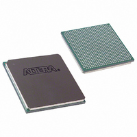
EP3C120F780C8N Altera, EP3C120F780C8N Datasheet - Page 40

EP3C120F780C8N
Manufacturer Part Number
EP3C120F780C8N
Description
IC CYCLONE III FPGA 119K 780FBGA
Manufacturer
Altera
Series
Cyclone® IIIr
Datasheets
1.EP3C5F256C8N.pdf
(5 pages)
2.EP3C5F256C8N.pdf
(34 pages)
3.EP3C5F256C8N.pdf
(66 pages)
4.EP3C5F256C8N.pdf
(14 pages)
5.EP3C5F256C8N.pdf
(76 pages)
6.EP3C120F780C8N.pdf
(274 pages)
Specifications of EP3C120F780C8N
Number Of Logic Elements/cells
119088
Number Of Labs/clbs
7443
Total Ram Bits
3981312
Number Of I /o
531
Voltage - Supply
1.15 V ~ 1.25 V
Mounting Type
Surface Mount
Operating Temperature
0°C ~ 85°C
Package / Case
780-FBGA
Family Name
Cyclone III
Number Of Logic Blocks/elements
119088
# I/os (max)
531
Frequency (max)
402MHz
Process Technology
65nm
Operating Supply Voltage (typ)
1.2V
Logic Cells
119088
Ram Bits
3981312
Operating Supply Voltage (min)
1.15V
Operating Supply Voltage (max)
1.25V
Operating Temp Range
0C to 85C
Operating Temperature Classification
Commercial
Mounting
Surface Mount
Pin Count
780
Package Type
FBGA
For Use With
544-2601 - KIT DEV CYCLONE III LS EP3CLS200544-2589 - KIT DEV EMB CYCLONE III EDITION544-2566 - KIT DEV DSP CYCLONE III EDITION544-2444 - KIT DEV CYCLONE III EP3C120544-2411 - KIT DEV NIOS II CYCLONE III ED.
Lead Free Status / RoHS Status
Lead free / RoHS Compliant
Number Of Gates
-
Lead Free Status / Rohs Status
Compliant
Other names
544-2392
544-2533
544-2533
EP3C120F780C8NES
544-2533
544-2533
EP3C120F780C8NES
Available stocks
Company
Part Number
Manufacturer
Quantity
Price
Company:
Part Number:
EP3C120F780C8N
Manufacturer:
ALTERA
Quantity:
642
Part Number:
EP3C120F780C8N
Manufacturer:
ALTERA/阿尔特拉
Quantity:
20 000
3–4
Byte Enable Support
Cyclone III Device Handbook, Volume 1
The Cyclone III device family M9K memory blocks support byte enables that mask
the input data so that only specific bytes of data are written. The unwritten bytes
retain the previous written value. The wren signals, along with the byte-enable
(byteena) signals, control the write operations of the RAM block. The default value
of the byteena signals is high (enabled), in which case writing is controlled only by
the wren signals. There is no clear port to the byteena registers. M9K blocks support
byte enables when the write port has a data width of ×16, ×18, ×32, or ×36 bits.
Byte enables operate in one-hot manner, with the LSB of the byteena signal
corresponding to the least significant byte of the data bus. For example, if
byteena = 01 and you are using a RAM block in ×18 mode, data[8..0] is
enabled and data[17..9] is disabled. Similarly, if byteena = 11, both
data[8..0] and data[17..9] are enabled. Byte enables are active high.
Table 3–2
Table 3–2. byteena for Cyclone III Device Family M9K Blocks
Note to
(1) Any combination of byte enables is possible.
byteena[3..0]
[0] = 1
[1] = 1
[2] = 1
[3] = 1
Table
lists the byte selection.
3–2:
datain
[15..8]
[7..0]
—
—
× 16
datain
[17..9]
[8..0]
—
—
Chapter 3: Memory Blocks in the Cyclone III Device Family
× 18
Affected Bytes
datain
(Note 1)
[23..16]
[31..24]
[15..8]
[7..0]
© December 2009 Altera Corporation
× 32
datain
[26..18]
[35..27]
[17..9]
[8..0]
× 36
Overview


