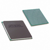
EP1SGX25CF672C6 Altera, EP1SGX25CF672C6 Datasheet - Page 102

EP1SGX25CF672C6
Manufacturer Part Number
EP1SGX25CF672C6
Description
IC STRATIX GX FPGA 25KLE 672FBGA
Manufacturer
Altera
Series
Stratix® GXr
Datasheet
1.EP1SGX10CF672C7N.pdf
(272 pages)
Specifications of EP1SGX25CF672C6
Number Of Logic Elements/cells
25660
Number Of Labs/clbs
2566
Total Ram Bits
1944576
Number Of I /o
455
Voltage - Supply
1.425 V ~ 1.575 V
Mounting Type
Surface Mount
Operating Temperature
0°C ~ 85°C
Package / Case
672-FBGA
Family Name
Stratix GX
Number Of Logic Blocks/elements
25660
# I/os (max)
455
Frequency (max)
5GHz
Process Technology
SRAM
Operating Supply Voltage (typ)
1.5V
Logic Cells
25660
Ram Bits
1944576
Operating Supply Voltage (min)
1.425V
Operating Supply Voltage (max)
1.575V
Operating Temp Range
0C to 85C
Operating Temperature Classification
Commercial
Mounting
Surface Mount
Pin Count
672
Package Type
FC-FBGA
Lead Free Status / RoHS Status
Contains lead / RoHS non-compliant
Number Of Gates
-
Lead Free Status / Rohs Status
Not Compliant
Available stocks
Company
Part Number
Manufacturer
Quantity
Price
Company:
Part Number:
EP1SGX25CF672C6
Manufacturer:
ALTERA
Quantity:
3 000
Part Number:
EP1SGX25CF672C6
Manufacturer:
ALTERA/阿尔特拉
Quantity:
20 000
Company:
Part Number:
EP1SGX25CF672C6ES
Manufacturer:
ALTERA
Quantity:
5
- Current page: 102 of 272
- Download datasheet (3Mb)
TriMatrix Memory
Figure 4–20. Left-Facing M-RAM to Interconnect Interface
Notes to
(1)
(2)
4–36
Stratix GX Device Handbook, Volume 1
Only R24 and C16 interconnects cross the M-RAM block boundaries.
The right-facing M-RAM block has interface blocks on the right side, but none on the left. B1 to B6 and A1 to A6
orientation is clipped across the vertical axis for right-facing M-RAM blocks.
Figure
4–20:
Row Unit Interface
Allows LAB Rows to
Drive Address and
Control Signals to
M-RAM Block
LABs in Row
M-RAM Boundary
R11
R10
R9
R8
R7
R6
R5
R4
R3
R2
R1
LAB Interface
Blocks
M512 RAM Block Columns
B1
A1
B2
A2
M-RAM Block
B3
A3
Port B
Port A
B4
A4
Notes
(1),
B5
A5
(2)
B6
A6
Column Interface Block
Allows LAB Columns to
Drive datain and dataout to
and from M-RAM Block
LABs in Column
M-RAM Boundary
Column Interface Block
Drives to and from
C4 and C8 Interconnects
Altera Corporation
February 2005
Related parts for EP1SGX25CF672C6
Image
Part Number
Description
Manufacturer
Datasheet
Request
R

Part Number:
Description:
CYCLONE II STARTER KIT EP2C20N
Manufacturer:
Altera
Datasheet:

Part Number:
Description:
CPLD, EP610 Family, ECMOS Process, 300 Gates, 16 Macro Cells, 16 Reg., 16 User I/Os, 5V Supply, 35 Speed Grade, 24DIP
Manufacturer:
Altera Corporation
Datasheet:

Part Number:
Description:
CPLD, EP610 Family, ECMOS Process, 300 Gates, 16 Macro Cells, 16 Reg., 16 User I/Os, 5V Supply, 15 Speed Grade, 24DIP
Manufacturer:
Altera Corporation
Datasheet:

Part Number:
Description:
Manufacturer:
Altera Corporation
Datasheet:

Part Number:
Description:
CPLD, EP610 Family, ECMOS Process, 300 Gates, 16 Macro Cells, 16 Reg., 16 User I/Os, 5V Supply, 30 Speed Grade, 24DIP
Manufacturer:
Altera Corporation
Datasheet:

Part Number:
Description:
High-performance, low-power erasable programmable logic devices with 8 macrocells, 10ns
Manufacturer:
Altera Corporation
Datasheet:

Part Number:
Description:
High-performance, low-power erasable programmable logic devices with 8 macrocells, 7ns
Manufacturer:
Altera Corporation
Datasheet:

Part Number:
Description:
Classic EPLD
Manufacturer:
Altera Corporation
Datasheet:

Part Number:
Description:
High-performance, low-power erasable programmable logic devices with 8 macrocells, 10ns
Manufacturer:
Altera Corporation
Datasheet:

Part Number:
Description:
Manufacturer:
Altera Corporation
Datasheet:

Part Number:
Description:
Manufacturer:
Altera Corporation
Datasheet:

Part Number:
Description:
Manufacturer:
Altera Corporation
Datasheet:

Part Number:
Description:
CPLD, EP610 Family, ECMOS Process, 300 Gates, 16 Macro Cells, 16 Reg., 16 User I/Os, 5V Supply, 25 Speed Grade, 24DIP
Manufacturer:
Altera Corporation
Datasheet:


