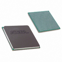
EP1SGX25CF672C6 Altera, EP1SGX25CF672C6 Datasheet - Page 34

EP1SGX25CF672C6
Manufacturer Part Number
EP1SGX25CF672C6
Description
IC STRATIX GX FPGA 25KLE 672FBGA
Manufacturer
Altera
Series
Stratix® GXr
Datasheet
1.EP1SGX10CF672C7N.pdf
(272 pages)
Specifications of EP1SGX25CF672C6
Number Of Logic Elements/cells
25660
Number Of Labs/clbs
2566
Total Ram Bits
1944576
Number Of I /o
455
Voltage - Supply
1.425 V ~ 1.575 V
Mounting Type
Surface Mount
Operating Temperature
0°C ~ 85°C
Package / Case
672-FBGA
Family Name
Stratix GX
Number Of Logic Blocks/elements
25660
# I/os (max)
455
Frequency (max)
5GHz
Process Technology
SRAM
Operating Supply Voltage (typ)
1.5V
Logic Cells
25660
Ram Bits
1944576
Operating Supply Voltage (min)
1.425V
Operating Supply Voltage (max)
1.575V
Operating Temp Range
0C to 85C
Operating Temperature Classification
Commercial
Mounting
Surface Mount
Pin Count
672
Package Type
FC-FBGA
Lead Free Status / RoHS Status
Contains lead / RoHS non-compliant
Number Of Gates
-
Lead Free Status / Rohs Status
Not Compliant
Available stocks
Company
Part Number
Manufacturer
Quantity
Price
Company:
Part Number:
EP1SGX25CF672C6
Manufacturer:
ALTERA
Quantity:
3 000
Part Number:
EP1SGX25CF672C6
Manufacturer:
ALTERA/阿尔特拉
Quantity:
20 000
Company:
Part Number:
EP1SGX25CF672C6ES
Manufacturer:
ALTERA
Quantity:
5
2–24
Stratix GX Device Handbook, Volume 1
XAUI Mode
In XAUI mode, the rate matcher adheres to clause 48 of the IEEE 802.3ae
specification for clock rate compensation. The rate matcher performs
clock compensation on columns of /R/ (/K28.0/), denoted by //R//.
An //R// is added or deleted automatically based on the number of
words in the FIFO buffer.
8B/10B Decoder
The 8B/10B decoder converts the 10-bit encoded code group into 8-bit
data and 1 control bit. The 8B/10B decoder can be bypassed. The
following is a diagram of the conversion from a 10-bit encoded code
group into 8-bit data + 1-bit control.
Figure 2–20. 8B/10B Decoder Conversion
There are two optional error status ports available in the 8B/10B decoder,
rx_errdetect and rx_disperr.
ports from a given error. These status signals are aligned with the code
group in which the error occurred.
No errors
Invalid code groups
Disparity errors
Table 2–7. Error Signal Values
Types of Errors
Parallel data
MSB received last
9
j
h
8
H
7
g
7
G
6
rx_errdetect
8b-10b conversion
6
5
F
f
1’b0
1’b1
1’b1
E
4
5
i
Table 2–7
D
3
e
4
2
C
d
3
shows the values of the
1
B
c
2
LSB received first
0
A
b
1
rx_disperr
Altera Corporation
+
1’b0
1’b0
1’b1
a
0
ctrl
June 2006


