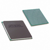
EP1SGX25CF672C6 Altera, EP1SGX25CF672C6 Datasheet - Page 52

EP1SGX25CF672C6
Manufacturer Part Number
EP1SGX25CF672C6
Description
IC STRATIX GX FPGA 25KLE 672FBGA
Manufacturer
Altera
Series
Stratix® GXr
Datasheet
1.EP1SGX10CF672C7N.pdf
(272 pages)
Specifications of EP1SGX25CF672C6
Number Of Logic Elements/cells
25660
Number Of Labs/clbs
2566
Total Ram Bits
1944576
Number Of I /o
455
Voltage - Supply
1.425 V ~ 1.575 V
Mounting Type
Surface Mount
Operating Temperature
0°C ~ 85°C
Package / Case
672-FBGA
Family Name
Stratix GX
Number Of Logic Blocks/elements
25660
# I/os (max)
455
Frequency (max)
5GHz
Process Technology
SRAM
Operating Supply Voltage (typ)
1.5V
Logic Cells
25660
Ram Bits
1944576
Operating Supply Voltage (min)
1.425V
Operating Supply Voltage (max)
1.575V
Operating Temp Range
0C to 85C
Operating Temperature Classification
Commercial
Mounting
Surface Mount
Pin Count
672
Package Type
FC-FBGA
Lead Free Status / RoHS Status
Contains lead / RoHS non-compliant
Number Of Gates
-
Lead Free Status / Rohs Status
Not Compliant
Available stocks
Company
Part Number
Manufacturer
Quantity
Price
Company:
Part Number:
EP1SGX25CF672C6
Manufacturer:
ALTERA
Quantity:
3 000
Part Number:
EP1SGX25CF672C6
Manufacturer:
ALTERA/阿尔特拉
Quantity:
20 000
Company:
Part Number:
EP1SGX25CF672C6ES
Manufacturer:
ALTERA
Quantity:
5
Introduction
3–2
Stratix GX Device Handbook, Volume 1
multiplication value. The
bypassing the SERDES. The SERDES DPA cannot support
natively.
On the receiver side, the high-frequency clock generated by the PLL shifts
the serial data through a shift register (also called deserializer). The
parallel data is clocked out to the logic array synchronized with the low-
frequency clock. On the transmitter side, the parallel data from the logic
array is first clocked into a parallel-in, serial-out shift register
synchronized with the low-frequency clock and then transmitted out by
the output buffers.
There are two dedicated fast PLLs each in EP1SGX10 to EP1SGX25
devices, and four in EP1SGX40 devices. These PLLs are used for the
SERDES operations as well as general-purpose use.
Stratix GX Differential I/O Receiver Operation (Non-DPA Mode)
You can configure any of the Stratix GX source synchronous differential
input channels as a receiver channel (see
receiver deserializes the incoming high-speed data. The input shift
register continuously clocks the incoming data on the negative transition
of the high-frequency clock generated by the PLL clock (
The data in the serial shift register is shifted into a parallel register by the
RXLOADEN signal generated by the fast PLL counter circuitry on the third
falling edge of the high-frequency clock. However, you can select which
falling edge of the high frequency clock loads the data into the parallel
register, using the data-realignment circuit.
In normal mode, the enable signal RXLOADEN loads the parallel data into
the next parallel register on the second rising edge of the low-frequency
clock. You can also load data to the parallel register through the
TXLOADEN signal when using the data-realignment circuit.
Figure 3–1
Figure 3–2
Stratix GX devices in
is the data parallelization division factor.
shows the block diagram of a single SERDES receiver channel.
shows the timing relationship between the data and clocks in
×
10 mode. W is the low-frequency multiplier and J
×
1 and
×
2 operation is also possible by
Figure
3–1). The differential
Altera Corporation
×
W).
×
1,
August 2005
×
2
, or ×
4


