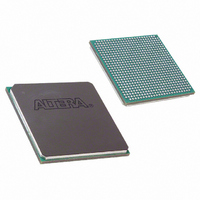
EP1SGX25CF672C6 Altera, EP1SGX25CF672C6 Datasheet - Page 228

EP1SGX25CF672C6
Manufacturer Part Number
EP1SGX25CF672C6
Description
IC STRATIX GX FPGA 25KLE 672FBGA
Manufacturer
Altera
Series
Stratix® GXr
Datasheet
1.EP1SGX10CF672C7N.pdf
(272 pages)
Specifications of EP1SGX25CF672C6
Number Of Logic Elements/cells
25660
Number Of Labs/clbs
2566
Total Ram Bits
1944576
Number Of I /o
455
Voltage - Supply
1.425 V ~ 1.575 V
Mounting Type
Surface Mount
Operating Temperature
0°C ~ 85°C
Package / Case
672-FBGA
Family Name
Stratix GX
Number Of Logic Blocks/elements
25660
# I/os (max)
455
Frequency (max)
5GHz
Process Technology
SRAM
Operating Supply Voltage (typ)
1.5V
Logic Cells
25660
Ram Bits
1944576
Operating Supply Voltage (min)
1.425V
Operating Supply Voltage (max)
1.575V
Operating Temp Range
0C to 85C
Operating Temperature Classification
Commercial
Mounting
Surface Mount
Pin Count
672
Package Type
FC-FBGA
Lead Free Status / RoHS Status
Contains lead / RoHS non-compliant
Number Of Gates
-
Lead Free Status / Rohs Status
Not Compliant
Available stocks
Company
Part Number
Manufacturer
Quantity
Price
Company:
Part Number:
EP1SGX25CF672C6
Manufacturer:
ALTERA
Quantity:
3 000
Part Number:
EP1SGX25CF672C6
Manufacturer:
ALTERA/阿尔特拉
Quantity:
20 000
Company:
Part Number:
EP1SGX25CF672C6ES
Manufacturer:
ALTERA
Quantity:
5
Timing Model
6–26
Stratix GX Device Handbook, Volume 1
Internal Timing Parameters
Internal timing parameters are specified on a speed grade basis
independent of device density.
Stratix GX device internal timing microparameters for LEs, IOEs,
TriMatrix
interconnects.
t
t
t
t
t
t
t
t
t
t
t
t
t
t
t
t
t
SU
H
CO
LUT
CLR
PRE
CLKHL
SU
H
CO
PIN2COMBOUT_R
PIN2COMBOUT_C
COMBIN2PIN_R
COMBIN2PIN_C
CLR
PRE
CLKHL
Table 6–36. LE Internal Timing Microparameter Descriptions
Table 6–37. IOE Internal Timing Microparameter Descriptions
Symbol
Symbol
™
memory structures, DSP blocks, and MultiTrack
LE register setup time before clock
LE register hold time after clock
LE register clock-to-output delay
LE combinational LUT delay for data-in to data-out
Minimum clear pulse width
Minimum preset pulse width
Minimum clock high or low time
IOE input and output register setup time before clock
IOE input and output register hold time after clock
IOE input and output register clock-to-output delay
Row input pin to IOE combinational output
Column input pin to IOE combinational output
Row IOE data input to combinational output pin
Column IOE data input to combinational output pin
Minimum clear pulse width
Minimum preset pulse width
Minimum clock high or low time
Tables 6–36
Parameter
Parameter
through
6–42
Altera Corporation
describe the
June 2006


