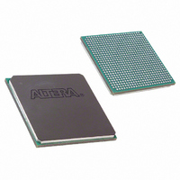
EP1SGX25CF672C6 Altera, EP1SGX25CF672C6 Datasheet - Page 132

EP1SGX25CF672C6
Manufacturer Part Number
EP1SGX25CF672C6
Description
IC STRATIX GX FPGA 25KLE 672FBGA
Manufacturer
Altera
Series
Stratix® GXr
Datasheet
1.EP1SGX10CF672C7N.pdf
(272 pages)
Specifications of EP1SGX25CF672C6
Number Of Logic Elements/cells
25660
Number Of Labs/clbs
2566
Total Ram Bits
1944576
Number Of I /o
455
Voltage - Supply
1.425 V ~ 1.575 V
Mounting Type
Surface Mount
Operating Temperature
0°C ~ 85°C
Package / Case
672-FBGA
Family Name
Stratix GX
Number Of Logic Blocks/elements
25660
# I/os (max)
455
Frequency (max)
5GHz
Process Technology
SRAM
Operating Supply Voltage (typ)
1.5V
Logic Cells
25660
Ram Bits
1944576
Operating Supply Voltage (min)
1.425V
Operating Supply Voltage (max)
1.575V
Operating Temp Range
0C to 85C
Operating Temperature Classification
Commercial
Mounting
Surface Mount
Pin Count
672
Package Type
FC-FBGA
Lead Free Status / RoHS Status
Contains lead / RoHS non-compliant
Number Of Gates
-
Lead Free Status / Rohs Status
Not Compliant
Available stocks
Company
Part Number
Manufacturer
Quantity
Price
Company:
Part Number:
EP1SGX25CF672C6
Manufacturer:
ALTERA
Quantity:
3 000
Part Number:
EP1SGX25CF672C6
Manufacturer:
ALTERA/阿尔特拉
Quantity:
20 000
Company:
Part Number:
EP1SGX25CF672C6ES
Manufacturer:
ALTERA
Quantity:
5
Digital Signal Processing Block
4–66
Stratix GX Device Handbook, Volume 1
The DSP block is divided into eight block units that interface with eight
LAB rows on the left and right. Each block unit can be considered half of
an 18
interconnect region is associated with each DSP block. Like an LAB, this
interconnect region can be fed with 10 direct link interconnects from the
LAB to the left or right of the DSP block in the same row. All row and
column routing resources can access the DSP block’s local interconnect
region. The outputs also work similarly to LAB outputs as well. Nine
outputs from the DSP block can drive to the left LAB through direct link
interconnects and nine can drive to the right LAB though direct link
interconnects. All 18 outputs can drive to all types of row and column
routing. Outputs can drive right- or left-column routing.
and
Figure 4–39. DSP Block Interconnect Interface
4–40
×
18-bit multiplier sub-block with 18 inputs and 18 outputs. A local
Interconnect
show the DSP block interfaces to LAB rows.
MultiTrack
B1[17..0]
A2[17..0]
B2[17..0]
A3[17..0]
B3[17..0]
A4[17..0]
B4[17..0]
A1[17..0]
DSP Block
OG[17..0]
OB[17..0]
OC[17..0]
OD[17..0]
OE[17..0]
OH[17..0]
OA[17..0]
OF[17..0]
MultiTrack
Interconnect
Altera Corporation
Figures 4–39
February 2005


