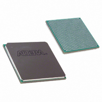
EP1SGX25CF672C6 Altera, EP1SGX25CF672C6 Datasheet - Page 260

EP1SGX25CF672C6
Manufacturer Part Number
EP1SGX25CF672C6
Description
IC STRATIX GX FPGA 25KLE 672FBGA
Manufacturer
Altera
Series
Stratix® GXr
Datasheet
1.EP1SGX10CF672C7N.pdf
(272 pages)
Specifications of EP1SGX25CF672C6
Number Of Logic Elements/cells
25660
Number Of Labs/clbs
2566
Total Ram Bits
1944576
Number Of I /o
455
Voltage - Supply
1.425 V ~ 1.575 V
Mounting Type
Surface Mount
Operating Temperature
0°C ~ 85°C
Package / Case
672-FBGA
Family Name
Stratix GX
Number Of Logic Blocks/elements
25660
# I/os (max)
455
Frequency (max)
5GHz
Process Technology
SRAM
Operating Supply Voltage (typ)
1.5V
Logic Cells
25660
Ram Bits
1944576
Operating Supply Voltage (min)
1.425V
Operating Supply Voltage (max)
1.575V
Operating Temp Range
0C to 85C
Operating Temperature Classification
Commercial
Mounting
Surface Mount
Pin Count
672
Package Type
FC-FBGA
Lead Free Status / RoHS Status
Contains lead / RoHS non-compliant
Number Of Gates
-
Lead Free Status / Rohs Status
Not Compliant
Available stocks
Company
Part Number
Manufacturer
Quantity
Price
Company:
Part Number:
EP1SGX25CF672C6
Manufacturer:
ALTERA
Quantity:
3 000
Part Number:
EP1SGX25CF672C6
Manufacturer:
ALTERA/阿尔特拉
Quantity:
20 000
Company:
Part Number:
EP1SGX25CF672C6ES
Manufacturer:
ALTERA
Quantity:
5
High-Speed I/O Specification
High-Speed I/O
Specification
6–58
Stratix GX Device Handbook, Volume 1
1.5 V
LVCMOS
GTL
GTL+
SSTL-3 class I
SSTL-3 class II
SSTL-2 class I
SSTL-2 class II
SSTL-18 class I
SSTL-18 class II
HSTL class I
HSTL class II
3.3-V PCI
3.3-V PCI-X 1.0
Compact PCI
AGP 1×
AGP 2×
CTT
Differential HSTL
LVDS
LVPECL
PCML
HyperTransport technology
t
f
t
C
HSCLK
RISE
Table 6–85. Stratix GX Maximum Output Clock Rate (Using I/O Pins) for PLL[1, 2] Pins (Part 2 of 2)
Table 6–86. High-Speed Timing Specifications & Definitions (Part 1 of 2)
High-Speed Timing Specification
I/O Standard
Table 6–86
High-speed receiver/transmitter input and output clock period.
High-speed receiver/transmitter input and output clock frequency.
Low-to-high transmission time.
provides high-speed timing specifications definitions.
-5 Speed Grade -6 Speed Grade -7 Speed Grade
400
250
225
225
400
225
717
420
350
200
200
167
167
150
150
150
150
250
400
400
300
717
420
300
350
167
167
150
150
133
133
133
133
225
225
225
225
350
350
350
250
225
717
717
420
420
Definitions
300
300
125
125
133
133
133
133
133
133
200
200
200
200
300
300
300
200
200
500
500
420
420
Altera Corporation
June 2006
MHz
MHz
MHz
MHz
MHz
MHz
MHz
MHz
MHz
MHz
MHz
MHz
MHz
MHz
MHz
MHz
MHz
MHz
MHz
MHz
MHz
MHz
MHz
Unit


