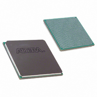
EP1SGX25CF672C6 Altera, EP1SGX25CF672C6 Datasheet - Page 148

EP1SGX25CF672C6
Manufacturer Part Number
EP1SGX25CF672C6
Description
IC STRATIX GX FPGA 25KLE 672FBGA
Manufacturer
Altera
Series
Stratix® GXr
Datasheet
1.EP1SGX10CF672C7N.pdf
(272 pages)
Specifications of EP1SGX25CF672C6
Number Of Logic Elements/cells
25660
Number Of Labs/clbs
2566
Total Ram Bits
1944576
Number Of I /o
455
Voltage - Supply
1.425 V ~ 1.575 V
Mounting Type
Surface Mount
Operating Temperature
0°C ~ 85°C
Package / Case
672-FBGA
Family Name
Stratix GX
Number Of Logic Blocks/elements
25660
# I/os (max)
455
Frequency (max)
5GHz
Process Technology
SRAM
Operating Supply Voltage (typ)
1.5V
Logic Cells
25660
Ram Bits
1944576
Operating Supply Voltage (min)
1.425V
Operating Supply Voltage (max)
1.575V
Operating Temp Range
0C to 85C
Operating Temperature Classification
Commercial
Mounting
Surface Mount
Pin Count
672
Package Type
FC-FBGA
Lead Free Status / RoHS Status
Contains lead / RoHS non-compliant
Number Of Gates
-
Lead Free Status / Rohs Status
Not Compliant
Available stocks
Company
Part Number
Manufacturer
Quantity
Price
Company:
Part Number:
EP1SGX25CF672C6
Manufacturer:
ALTERA
Quantity:
3 000
Part Number:
EP1SGX25CF672C6
Manufacturer:
ALTERA/阿尔特拉
Quantity:
20 000
Company:
Part Number:
EP1SGX25CF672C6ES
Manufacturer:
ALTERA
Quantity:
5
PLLs & Clock Networks
Figure 4–51. Stratix GX Enhanced PLL
Notes to
(1)
(2)
(3)
4–82
Stratix GX Device Handbook, Volume 1
CLK0
CLK1
External feedback is available in PLLs 5 and 6.
This external output is available from the g0 counter for PLLs 11 and 12.
These counters and external outputs are available in PLLs 5 and 6.
Figure
Switch-Over
Circuitry
Clock
4–51:
FBIN
/n
(1)
Δt
Enhanced PLLs
Stratix GX devices contain up to four enhanced PLLs with advanced
clock management features.
enhanced PLL.
Phase Frequency
Detector
PFD
Charge
Pump
VCO Phase Selection
Selectable at Each
PLL Output Port
Lock Detect
& Filter
VCO Phase Selection
Affecting All Outputs
Spectrum
Δt
Spread
Filter
Loop
/m
From Adjacent PLL
VCO
Figure 4–51
8
Post-Scale
Counters
shows a diagram of the
/g0
/g1
/g2
/g3
/e0
/e1
/e2
/e3
/l0
/l1
Δt
Δt
Δt
Δt
Δt
Δt
Δt
Δt
Δt
Δt
Programmable
Time Delay on
Each PLL Port
4
4
Altera Corporation
February 2005
I/O Buffers (2)
to I/O or general
routing
Regional
Clocks
Global
Clocks
I/O Buffers (3)


