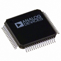
ADE7166ASTZF8 Analog Devices Inc, ADE7166ASTZF8 Datasheet - Page 104

ADE7166ASTZF8
Manufacturer Part Number
ADE7166ASTZF8
Description
IC ENERGY METER 1PHASE 64LQFP
Manufacturer
Analog Devices Inc
Specifications of ADE7166ASTZF8
Applications
Energy Measurement
Core Processor
8052
Program Memory Type
FLASH (8 kB)
Controller Series
ADE71xx
Ram Size
512 x 8
Interface
I²C, SPI, UART
Number Of I /o
20
Voltage - Supply
3.135 V ~ 3.465 V
Operating Temperature
-40°C ~ 85°C
Mounting Type
Surface Mount
Package / Case
64-LQFP
Ic Function
Single Phase Energy Measurement IC
Supply Voltage Range
3.13V To 3.46V, 2.4V To 3.7V
Operating Temperature Range
-40°C To +85°C
Digital Ic Case Style
LQFP
No. Of Pins
64
Lead Free Status / RoHS Status
Lead free / RoHS Compliant
Available stocks
Company
Part Number
Manufacturer
Quantity
Price
Company:
Part Number:
ADE7166ASTZF8
Manufacturer:
Analog Devices Inc
Quantity:
10 000
Company:
Part Number:
ADE7166ASTZF8-RL
Manufacturer:
Analog Devices Inc
Quantity:
10 000
ADE7566/ADE7569/ADE7166/ADE7169
FLASH MEMORY ORGANIZATION
The 16 kB of flash memory provided by the ADE7566/ADE7569/
ADE7166/ADE7169 are segmented into 32 pages of 512 bytes
each. It is up to the user to decide which flash memory to
allocate for data memory. It is recommended that each page be
dedicated solely to program memory or data memory. Doing so
prevents the program counter from being loaded with data
memory instead of an operations code from the program
memory. It also prevents program memory used to update a
byte of data memory from being erased.
The flash memory can be protected from read or write/erase
(W/E) access. The protection is implemented in part of the last
page of the flash memory, Page 31. Four of the bytes from this
page are used to set up write/erase protection for each page.
Another byte is used for configuring read protection of the flash
memory. The read protection is selected for groups of four pages.
Finally, one byte is used to store the key required for modifying
the protection scheme. The last page of flash memory must be
write/erase protected for any flash protection to be active.
0x3DFF
0x3BFF
0x2DFF
0x2BFF
0x3FFF
0x3E00
0x3C00
0x3A00
0x39FF
0x37FF
0x35FF
0x33FF
0x31FF
0x2FFF
0x2E00
0x2C00
0x2A00
0x29FF
0x27FF
0x25FF
0x23FF
0x21FF
0x3800
0x3600
0x3400
0x3200
0x3000
0x2800
0x2600
0x2400
0x2200
0x2000
CONTAINS PROTECTION SETTINGS.
PAGE 31
PAGE 30
PAGE 29
PAGE 28
PAGE 27
PAGE 26
PAGE 25
PAGE 24
PAGE 23
PAGE 22
PAGE 21
PAGE 20
PAGE 19
PAGE 18
PAGE 17
PAGE 16
Figure 92. Flash Memory Organization
READ
PROTECT
BIT 7
READ
PROTECT
BIT 6
READ
PROTECT
BIT 5
READ
PROTECT
BIT 4
0x1DFF
0x1BFF
0x0DFF
0x0BFF
0x1FFF
0x1C00
0x1A00
0x0FFF
0x0C00
0x0A00
0x1E00
0x19FF
0x17FF
0x15FF
0x13FF
0x11FF
0x0E00
0x09FF
0x07FF
0x05FF
0x03FF
0x01FF
0x1800
0x1600
0x1400
0x1200
0x1000
0x0800
0x0600
0x0400
0x0200
0x0000
EADRH
PROTECTION KEY
Figure 93. Flash Memory Read/Write/Erase Protection Block Diagram
PAGE 15
PAGE 14
PAGE 13
PAGE 12
PAGE 11
PAGE 10
PAGE 9
PAGE 8
PAGE 7
PAGE 6
PAGE 5
PAGE 4
PAGE 3
PAGE 2
PAGE 1
PAGE 0
FLSHKY
EADRL
ADDRESS
FLASH
READ
PROTECT
BIT 3
READ
PROTECT
BIT 2
READ
PROTECT
BIT 1
READ
PROTECT
BIT 0
DECODER
ADDRESS
FLSHKY = 0 × 3B?
COMMAND
Rev. A | Page 104 of 144
PROTECTION
DECODER
ECON
ALLOWED?
The implication of write/erase protecting the last page is that
the content of the 506 bytes in this page that are available to the
user must not change.
Thus, if code protection is enabled, it is recommended to use
this last page for program memory only (if the firmware does
not need to be updated in the field). If the firmware must be
protected and can be updated at a future date, the last page
should be used only for constants utilized by the program code.
Therefore, Page 0 through Page 30 are for general program and
data memory use. It is recommended that Page 31 be used for
constants or code that do not need to be updated. Note that the
last six bytes of Page 31 are reserved for protecting the flash
memory.
USING THE FLASH MEMORY
The 16 kB of flash memory are configured as 32 pages, each of
512 bytes. As with the other ADE7566/ADE7569/ADE7166/
ADE7169 peripherals, the interface to this memory space is via
a group of registers mapped in the SFR space (see Table 91).
A data register, EDATA, holds the byte of data to be accessed. The
byte of flash memory is addressed via the EADRH and EADRL
registers. Finally, ECON is an 8-bit control register that can be
written to with one of seven flash memory access commands to
trigger various read, write, erase, and verify functions.
Table 91. The Flash SFRs
SFR
ECON
FLSHKY
PROTKY
EDATA
PROTB0
PROTB1
PROTR
EADRL
EADRH
Figure 93 demonstrates the steps required for access to the flash
memory.
ACCESS
Address
0xB9
0xBA
0xBB
0xBC
0xBD
0xBE
0xBF
0xC6
0xC7
TRUE: ACCESS
FALSE: ACCESS
ALLOWED
ECON = 0
DENIED
ECON = 1
0xFF
0xFF
0x00
0x00
Default
0x00
0xFF
0x00
0xFF
0xFF
Bit Address-
able
No
No
No
No
No
No
No
No
No
Description
Flash Control.
Flash Key.
Flash Protection
Key.
Flash Data.
Flash W/E
Protection 0.
Flash W/E
Protection 1.
Flash Read
Protection.
Flash Low Byte
Address.
Flash High
Byte Address.


