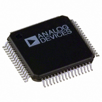
ADE7166ASTZF8 Analog Devices Inc, ADE7166ASTZF8 Datasheet - Page 46

ADE7166ASTZF8
Manufacturer Part Number
ADE7166ASTZF8
Description
IC ENERGY METER 1PHASE 64LQFP
Manufacturer
Analog Devices Inc
Specifications of ADE7166ASTZF8
Applications
Energy Measurement
Core Processor
8052
Program Memory Type
FLASH (8 kB)
Controller Series
ADE71xx
Ram Size
512 x 8
Interface
I²C, SPI, UART
Number Of I /o
20
Voltage - Supply
3.135 V ~ 3.465 V
Operating Temperature
-40°C ~ 85°C
Mounting Type
Surface Mount
Package / Case
64-LQFP
Ic Function
Single Phase Energy Measurement IC
Supply Voltage Range
3.13V To 3.46V, 2.4V To 3.7V
Operating Temperature Range
-40°C To +85°C
Digital Ic Case Style
LQFP
No. Of Pins
64
Lead Free Status / RoHS Status
Lead free / RoHS Compliant
Available stocks
Company
Part Number
Manufacturer
Quantity
Price
Company:
Part Number:
ADE7166ASTZF8
Manufacturer:
Analog Devices Inc
Quantity:
10 000
Company:
Part Number:
ADE7166ASTZF8-RL
Manufacturer:
Analog Devices Inc
Quantity:
10 000
ADE7566/ADE7569/ADE7166/ADE7169
Table 44. Interrupt Enable 3 SFR (MIRQENH, 0xDB)
Bit
7 to 6
5
4
3
2
1
0
ANALOG INPUTS
Each ADE7566/ADE7569/ADE7166/ADE7169 has two fully
differential voltage input channels. The maximum differential
input voltage for input pairs V
ADE7566 and ADE7569.
For the ADE7166 and ADE7169, PGA1 = 1 is not recommended
because at full scale, when both I
the ADC can be overranged. It is recommended, for these
products, that PGA1 = 2, 4, 8, or 16 be used.
Each analog input channel has a programmable gain amplifier
(PGA) with possible gain selections of 1, 2, 4, 8, and 16. The
gain selections are made by writing to the GAIN register (see
Table 37 and Figure 41). Bit 0 to Bit 2 select the gain for the PGA
in the current channel, and Bit 5 to Bit 7 select the gain for the
PGA in the voltage channel. For the ADE7166 and ADE7169, it
is recommended that PGA1 = 2, 4, 8, or 16 be used. Figure 40
shows how a gain selection for the current channel is made
using the gain register.
Interrupt Enable Bit
WFSM
PKI
PKV
CYCEND
ZXTO
ZX
P
/V
PA
N
and I
and I
Description
When this bit is set, the WFSM flag set creates a pending ADE interrupt to the 8052 core.
When this bit is set, the PKI flag set creates a pending ADE interrupt to the 8052 core.
When this bit is set, the PKV flag set creates a pending ADE interrupt to the 8052 core.
When this bit is set, the CYCEND flag set creates a pending ADE interrupt to the 8052 core.
When this bit is set, the ZXTO flag set creates a pending ADE interrupt to the 8052 core.
When this bit is set, the ZX flag set creates a pending ADE interrupt to the 8052 core.
Reserved.
PB
P
/I
are 180° out of phase,
N
is ±0.4 V. for the
Rev. A | Page 46 of 144
PGA2 GAIN SELECT
000 = × 1
001 = × 2
010 = × 4
011 = × 8
100 = × 16
*REGISTER CONTENTS SHOW POWER-ON DEFAULTS.
CURRENT AND VOLTAGE CHANNELS PGA CONTROL
V
V
V
IN
N
P
1
1
Figure 40. PGA in Current Channel
7
0
Figure 41. Analog Gain Register
7
0
6
0
6
0
GAIN REGISTER*
5
0
5
0
GAIN[7:0]
K × V
4
0
4
0
3
0
IN
3
0
2
0
CFSIGN_OPT
RESERVED
2
0
1
0
1
0
GAIN (K)
SELECTION
0
0
PGA1 GAIN SELECT
000 = × 1
001 = × 2
010 = × 4
011 = × 8
100 = × 16
0
0
ADDR:
0x1B


