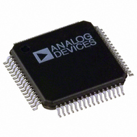
ADE7166ASTZF8 Analog Devices Inc, ADE7166ASTZF8 Datasheet - Page 107

ADE7166ASTZF8
Manufacturer Part Number
ADE7166ASTZF8
Description
IC ENERGY METER 1PHASE 64LQFP
Manufacturer
Analog Devices Inc
Specifications of ADE7166ASTZF8
Applications
Energy Measurement
Core Processor
8052
Program Memory Type
FLASH (8 kB)
Controller Series
ADE71xx
Ram Size
512 x 8
Interface
I²C, SPI, UART
Number Of I /o
20
Voltage - Supply
3.135 V ~ 3.465 V
Operating Temperature
-40°C ~ 85°C
Mounting Type
Surface Mount
Package / Case
64-LQFP
Ic Function
Single Phase Energy Measurement IC
Supply Voltage Range
3.13V To 3.46V, 2.4V To 3.7V
Operating Temperature Range
-40°C To +85°C
Digital Ic Case Style
LQFP
No. Of Pins
64
Lead Free Status / RoHS Status
Lead free / RoHS Compliant
Available stocks
Company
Part Number
Manufacturer
Quantity
Price
Company:
Part Number:
ADE7166ASTZF8
Manufacturer:
Analog Devices Inc
Quantity:
10 000
Company:
Part Number:
ADE7166ASTZF8-RL
Manufacturer:
Analog Devices Inc
Quantity:
10 000
PROTECTING THE FLASH MEMORY
Two forms of protection are offered for this flash memory: read
protection and write/erase protection. The read protection ensures
that any pages that are read protected are not able to be read by
the end user. The write protection ensures that the flash memory
cannot be erased or written over. This protects the end system
from tampering and can prevent the code from being overwritten
in the event of a unexpected disruption of the normal execution
of the program.
Write/erase protection is individually selectable for all 32 pages.
Read protection is selected in groups of 4 pages (see Figure 92
for the groupings). The protection bits are stored in the last
flash memory locations, Address 0x3FFA through Address
0x3FFF (see
protection, one byte is for read protection, and another byte sets
the protection security key. The user must enable read and
write/erase protection for the last page for the entire protection
scheme to work.
Note that the read protection does not prevent MOVC
commands from being executed within the code.
There is an additional layer of protection offered by a protection
security key. The user can set up this security key so that the
protection scheme cannot be changed without this key. Once
the protection key has been configured, it cannot be modified.
Enabling Flash Protection by Code
The protection bytes in the flash memory can be programmed
using the flash controller command and programming ECON to
0x08. In this case, the EADRH, EADRL, PROTB1, and PROTB0
bytes are used to store the data to be written to the 32 bits of
write protection. Note that the EADRH and EADRL registers
are not used as data pointers here but to store write protection
data.
PROTKY
PROTB1
PROTB0
EADRH
PROTR
EADRL
0x3FFD
0x3FFC
0x3FFF
0x3FFE
0x3FFB
0x3FFA
0x3FF9
0x3E00
Figure 94); four bytes are reserved for write/erase
Figure 94. Flash Protection in Page 31
WDOG
31:28
LOCK
WP
WP
WP
WP
RP
31
23
15
7
27:24
WP
WP
WP
WP
RP
30
22
14
6
23:20
WP
WP
WP
WP
RP
29
21
13
5
PROTECTION KEY
19:16
WP
WP
WP
WP
RP
28
20
12
4
15:12
WP
WP
WP
WP
RP
27
19
11
3
11:8
WP
WP
WP
WP
RP
26
18
10
2
WP
WP
WP
WP
7:4
RP
25
17
9
1
WP
WP
WP
WP
3:0
RP
24
16
8
0
Rev. A | Page 107 of 144
The sequence for writing the protection bits is as follows:
1.
2.
3.
4.
5.
To enable read and write/erase protection for the last page only,
use the following 8052 code. Writing the flash protection
command to the ECON register initiates programming of the
protection bits in the flash.
; enable read protection on the last four
pages only
MOV PROTR,#07Fh
; set up a protection key of 0A3h. This
command can be
; omitted to use the default protection key
of 0xFF
MOV PROTKY,#0A3h
; write the flash key to the FLSHKY register
to enable flash
; access. The flash access key is not
configurable.
MOV FLSHKY,#3Bh
; write flash protection command to the ECON
register
MOV ECON,#08h
ADE7566/ADE7569/ADE7166/ADE7169
Set up the EADRH, EADRL, PROTB1, and PROTB0
registers with the write/erase protection bits. When erased,
the protection bits default to 1 (like any other bit of flash
memory). The default protection setting is for no protection.
To enable protection, write a 0 to the bits corresponding to
the pages that should be protected.
Set up the PROTR register with the read protection bits.
Note that every read protection bit protects four pages.
To enable the read protection bit, write a 0 to the bits that
should be read protected.
To enable the protection key, write to the PROTKY register.
If enabled, the protection key is required to modify the
protection scheme. The protection key, Flash Memory
Address 0x3FFA, defaults to 0xFF; if the PROTKY register
is not written to, it remains 0xFF. If the protection key is
written to, the PROTKY register must be written with this
value every time the protection functionality is accessed.
Note that once the protection key is configured, it cannot
be modified. Also note that the most significant bit of
Address 0x3FFA is used to enable a lock mechanism for
the watchdog settings (see the
for more information).
Run the protection command by writing 0x08 to the
ECON register.
Reset the chip to activate the new protection.
Watchdog Timer section


