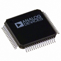
ADE7166ASTZF8 Analog Devices Inc, ADE7166ASTZF8 Datasheet - Page 128

ADE7166ASTZF8
Manufacturer Part Number
ADE7166ASTZF8
Description
IC ENERGY METER 1PHASE 64LQFP
Manufacturer
Analog Devices Inc
Specifications of ADE7166ASTZF8
Applications
Energy Measurement
Core Processor
8052
Program Memory Type
FLASH (8 kB)
Controller Series
ADE71xx
Ram Size
512 x 8
Interface
I²C, SPI, UART
Number Of I /o
20
Voltage - Supply
3.135 V ~ 3.465 V
Operating Temperature
-40°C ~ 85°C
Mounting Type
Surface Mount
Package / Case
64-LQFP
Ic Function
Single Phase Energy Measurement IC
Supply Voltage Range
3.13V To 3.46V, 2.4V To 3.7V
Operating Temperature Range
-40°C To +85°C
Digital Ic Case Style
LQFP
No. Of Pins
64
Lead Free Status / RoHS Status
Lead free / RoHS Compliant
Available stocks
Company
Part Number
Manufacturer
Quantity
Price
Company:
Part Number:
ADE7166ASTZF8
Manufacturer:
Analog Devices Inc
Quantity:
10 000
Company:
Part Number:
ADE7166ASTZF8-RL
Manufacturer:
Analog Devices Inc
Quantity:
10 000
ADE7566/ADE7569/ADE7166/ADE7169
SERIAL PERIPHERAL INTERFACE (SPI)
The ADE7566/ADE7569/ADE7166/ADE7169 integrate a
complete hardware serial peripheral interface on-chip. The SPI
is full duplex so that eight bits of data are synchronously
transmitted and simultaneously received. This SPI
implementation is double buffered, allowing users to read the
last byte of received data while a new byte is shifted in. The next
byte to be transmitted can be loaded while the current byte is
shifted out.
The SPI port can be configured for master or slave operation.
The physical interface to the SPI is via the MISO (P0.5),
MOSI (P0.4), SCLK (P0.6), and SS (P0.7) pins, while the
SPI REGISTERS
Table 137. SPI SFR List
SFR Address
0x9A
0x9B
0xE8
0xE9
0xEA
Table 138. SPI/I
Bit
7 to 0
Table 139. SPI/I
Bit
7 to 0
Mnemonic
SPI2CTx
Mnemonic
SPI2CRx
2
2
C Transmit Buffer SFR (SPI2CTx, 0x9A)
C Receive Buffer SFR (SPI2CRx, 0x9B)
Name
SPI2CTx
SPI2CRx
SPIMOD1
SPIMOD2
SPISTAT
Default
0
Default
0
Description
SPI or I
input. When a write is requested, the FIFO output is sent on the SPI or I
Description
SPI or I
to SPI2CRx SFR. A new data byte from the SPI or I
R/W
W
R
R/W
R/W
R/W
2
2
C Transmit Buffer. When SPI2CTx SFR is written, its content is transferred to the transmit FIFO
C Receive Buffer. When SPI2CRx SFR is read, one byte from the receive FIFO output is transferred
Length
8
8
8
8
8
Rev. A | Page 128 of 144
Default
0
0x10
0
0
firmware interface is via the SPI Configuration SFR 1
(SPIMOD1, 0xE8), the SPI Configuration SFR 2 (SPIMOD2,
0xE9), the SPI Interrupt Status SFR (SPISTAT, 0xEA), the
SPI/I
Receive Buffer SFR (SPI2CRx, 0x9B).
Note that the SPI pins are shared with the I
user can enable only one interface at a time. The SCPS bit in the
Configuration SFR (CFG, 0xAF) selects which peripheral is active.
2
C Transmit Buffer SFR (SPI2CTx, 0x9A), and the SPI/I
Description
SPI/I
SPI/I
SPI Configuration SFR 1 (see Table 140).
SPI Configuration SFR 2 (see Table 141).
SPI/I
2
C bus is written to the FIFO input.
2
2
2
C Transmit Buffer (see Table 138).
C Receive Buffer (see Table 139).
C Interrupt Status (see Table 142).
2
C bus.
2
C pins. Therefore, the
2
C


