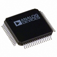
ADE7166ASTZF8 Analog Devices Inc, ADE7166ASTZF8 Datasheet - Page 134

ADE7166ASTZF8
Manufacturer Part Number
ADE7166ASTZF8
Description
IC ENERGY METER 1PHASE 64LQFP
Manufacturer
Analog Devices Inc
Specifications of ADE7166ASTZF8
Applications
Energy Measurement
Core Processor
8052
Program Memory Type
FLASH (8 kB)
Controller Series
ADE71xx
Ram Size
512 x 8
Interface
I²C, SPI, UART
Number Of I /o
20
Voltage - Supply
3.135 V ~ 3.465 V
Operating Temperature
-40°C ~ 85°C
Mounting Type
Surface Mount
Package / Case
64-LQFP
Ic Function
Single Phase Energy Measurement IC
Supply Voltage Range
3.13V To 3.46V, 2.4V To 3.7V
Operating Temperature Range
-40°C To +85°C
Digital Ic Case Style
LQFP
No. Of Pins
64
Lead Free Status / RoHS Status
Lead free / RoHS Compliant
Available stocks
Company
Part Number
Manufacturer
Quantity
Price
Company:
Part Number:
ADE7166ASTZF8
Manufacturer:
Analog Devices Inc
Quantity:
10 000
Company:
Part Number:
ADE7166ASTZF8-RL
Manufacturer:
Analog Devices Inc
Quantity:
10 000
ADE7566/ADE7569/ADE7166/ADE7169
I
The ADE7566/ADE7569/ADE7166/ADE7169 support a fully
licensed I
hardware master.
SDATA is the data I/O pin, and SCLK is the serial clock. These
two pins are shared with the MOSI and SCLK pins of the on-chip
SPI interface. Therefore, the user can enable only one interface
or the other on these pins at any given time. The SCPS bit in the
Configuration SFR (CFG, 0xAF) selects which peripheral is active.
The two pins used for data transfer, SDATA and SCLK, are
configured in a wire-AND format that allows arbitration in a
multimaster system.
The transfer sequence of an I
initiating a transfer by generating a start condition while the bus
is idle. The master transmits the address of the slave device and
the direction of the data transfer in the initial address transfer. If
the slave acknowledges, the data transfer is initiated. This continues
until the master issues a stop condition and the bus becomes idle.
SERIAL CLOCK GENERATION
The I
transfer. The master channel can be configured to operate in
fast mode (256 kHz) or standard mode (32 kHz).
Table 144. I
SFR Address
0x9A
0x9B
0xE8
0xE9
0xEA
Table 145. I
Bit
7
6 to 5
4 to 0
Table 146. I
Bit
7 to 1
0
2
C COMPATIBLE INTERFACE
2
C master in the system generates the serial clock for a
2
Address
0xEF
0xEE to 0xED
0xEC to 0xE8
Mnemonic
I2CSLVADR
I2CR_W
C interface. The I
2
2
2
C SFR List
C Mode SFR (I2CMOD, 0xE8)
C Slave Address SFR (I2CADR, 0xE9)
Name
SPI2CTx
SPI2CRx
I2CMOD
I2CADR
SPI2CSTAT
Mnemonic
I2CEN
I2CR[1:0]
I2CRCT[4:0]
Default
0
0
2
2
C interface is implemented as a full
C system consists of a master device
Description
Address of the I
Command Bit for Read or Write. When this bit is set to Logic 1, a read command is transmitted on the
I
to Logic 0, a write command is transmitted on the I
2
C bus. Data from the slave in the SPI2CRx SFR is expected after a command byte. When this bit is set
Default
0
0
0
R/W
W
R
R/W
R/W
R/W
Description
I
I2CADR SFR starts a communication.
I
I2CR[1:0]
00
01
10
11
Configures the length of the I
I2CRCT, Bit[4:0] + 1 byte have been read or if an error occurs.
2
2
C Enable Bit. When this bit is set to Logic 1, the I
C SCLK Frequency.
2
C Slave Being Addressed. Writing to this register starts the I
Length
8
8
8
8
8
Rev. A | Page 134 of 144
Result
f
f
f
f
CORE
CORE
CORE
CORE
/16 = 256 kHz if f
/32 = 128 kHz if f
/64 = 64 Hz if f
/128= 32 kHz if f
Default
0
0
0
0
The bit rate is defined in the I2CMOD SFR as follows:
SLAVE ADDRESSES
The I
device ID. The LSB of this register contains a read/write request.
A write to this SFR starts the I
I
The I
•
•
•
•
•
Because the SPI and I
they also share the same SFRs, such as the SPI2CTx and SPIXCRx
SFRs. In addition, the I2CMOD, I2CADR, SPI2CSTAT, and
SPI2CTx SFRs are shared with the SPIMOD1, SPIMOD2, and
SPISTAT SFRs, respectively.
2
C REGISTERS
I2CMOD
SPI2CSTAT
I2CADR
SPI2CTx
SPI2CRx
2
2
2
f
C received FIFO buffer. The I
C Slave Address SFR (I2CADR, 0xE9) contains the slave
C peripheral interface consists of five SFRs:
SCLK
CORE
CORE
CORE
CORE
= 4.096 MHz
=
= 4.096 MHz
= 4.096 MHz
= 4.096 MHz
2
16
C bus. Data to slave is expected in the SPI2CTx SFR.
Description
SPI/I
SPI/I
I
I
I
2
2
2
×
C Mode (see Table 145).
C Slave Address (see Table 146).
C Interrupt Status Register (see Table 147).
f
2
CORE
I
2
2
2
C Transmit Buffer (see Table 138).
C Receive Buffer (see Table 139).
CR
2
: 1 [
C serial interfaces share the same pins,
] 0
2
C interface is enabled. A write to the
2
C communication.
2
C peripheral stops when
2
C transmission (read or write).


