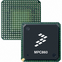
MC68MH360ZP33L Freescale Semiconductor, MC68MH360ZP33L Datasheet - Page 307

MC68MH360ZP33L
Manufacturer Part Number
MC68MH360ZP33L
Description
IC MPU 32BIT QUICC 357-PBGA
Manufacturer
Freescale Semiconductor
Specifications of MC68MH360ZP33L
Processor Type
M683xx 32-Bit
Speed
33MHz
Voltage
5V
Mounting Type
Surface Mount
Package / Case
357-PBGA
Lead Free Status / RoHS Status
Contains lead / RoHS non-compliant
Features
-
Available stocks
Company
Part Number
Manufacturer
Quantity
Price
Company:
Part Number:
MC68MH360ZP33L
Manufacturer:
FREESCALE
Quantity:
1 831
Company:
Part Number:
MC68MH360ZP33L
Manufacturer:
MOTOLOLA
Quantity:
672
Company:
Part Number:
MC68MH360ZP33L
Manufacturer:
Freescale Semiconductor
Quantity:
10 000
Part Number:
MC68MH360ZP33L
Manufacturer:
FREESCALE
Quantity:
20 000
Company:
Part Number:
MC68MH360ZP33LR2
Manufacturer:
Freescale Semiconductor
Quantity:
10 000
- Current page: 307 of 962
- Download datasheet (5Mb)
6.12.6 DRAM Bank External Master Support
The DRAM controller supports an external MC68EC040 as well as external MC68030-type
masters, including an external QUICC.
Whenever an external master is supported, external address multiplexing must be provided
by the user. The DRAM controller controls the multiplexing with the AMUX pin. On a normal
access, AMUX defaults high, and the upper address lines (row) should be multiplexed to the
DRAM first. After the external master outputs the full address, it asserts the AS/TS signal to
the QUICC. The DRAM controller then performs the address comparison, detects that the
access is to one of its DRAM banks, and issues the corresponding RAS signal. After the
assertion of the RAS signal, the DRAM controller continues the access and negates the
AMUX signal, controls the CAS and RAS timing, and generates the DSACK/TA signals to
terminate the access. Refer to Section 9 Applications for a description of an external master
system.
The DRAM controller supports the MC68EC040 in an optimized way. The DRAM controller
supports burst accesses made by an external MC68EC040 (or other M68040 family mem-
ber) if the BACK40 bit is set in the BR. The MC68EC040 requests a burst to be performed
with a line-fill indication on the SIZx (SIZ = 11) and TTx pins. In this case, the DRAM con-
troller performs a normal access (RAS and CAS), followed by requests to the DRAM for the
next three sequential long-word operands (CAS only). The DRAM controller automatically
increments the addresses to the DRAM using the BADDR3–BADDR2 pins.
6.12.7 Double-Drive RAS Lines
RAS1 and RAS2 have a special capability. To increase the available drive strength of these
pins, the RAS1 and RAS2 signals may be output simultaneously on two pins each. The extra
signals, called RAS1DD and RAS2DD, increase the effective drive strength of the RAS sig-
nals. This selection is made in the PEPAR.
6.12.8 DRAM Bus Error
The BERR signal may be asserted by the DRAM controller in the case of a parity error or by
the bus monitor of the SIM60 as a result of a write-protect violation. In addition, if the BERR
signal is asserted externally, it should not be asserted until at least S2 of the bus cycle if TSS
= 0 in the GMR, and until at least S4 of the bus cycle if TSS = 1 in the GMR.
MOTOROLA
user can either perform the reads in software or wait for the
DRAM refresh controller to perform these reads.
To support the MC68030 cache fill operations, the DRAM con-
troller asserts all four CAS signals during every QUICC/
MC68030-type external master read cycle to a DRAM bank.
(This includes byte or word reads by the MC68030.)
Freescale Semiconductor, Inc.
For More Information On This Product,
MC68360 USER’S MANUAL
Go to: www.freescale.com
NOTE
System Integration Module (SIM60)
6-63
Related parts for MC68MH360ZP33L
Image
Part Number
Description
Manufacturer
Datasheet
Request
R
Part Number:
Description:
Manufacturer:
Freescale Semiconductor, Inc
Datasheet:
Part Number:
Description:
Manufacturer:
Freescale Semiconductor, Inc
Datasheet:
Part Number:
Description:
Manufacturer:
Freescale Semiconductor, Inc
Datasheet:
Part Number:
Description:
Manufacturer:
Freescale Semiconductor, Inc
Datasheet:
Part Number:
Description:
Manufacturer:
Freescale Semiconductor, Inc
Datasheet:
Part Number:
Description:
Manufacturer:
Freescale Semiconductor, Inc
Datasheet:
Part Number:
Description:
Manufacturer:
Freescale Semiconductor, Inc
Datasheet:
Part Number:
Description:
Manufacturer:
Freescale Semiconductor, Inc
Datasheet:
Part Number:
Description:
Manufacturer:
Freescale Semiconductor, Inc
Datasheet:
Part Number:
Description:
Manufacturer:
Freescale Semiconductor, Inc
Datasheet:
Part Number:
Description:
Manufacturer:
Freescale Semiconductor, Inc
Datasheet:
Part Number:
Description:
Manufacturer:
Freescale Semiconductor, Inc
Datasheet:
Part Number:
Description:
Manufacturer:
Freescale Semiconductor, Inc
Datasheet:
Part Number:
Description:
Manufacturer:
Freescale Semiconductor, Inc
Datasheet:
Part Number:
Description:
Manufacturer:
Freescale Semiconductor, Inc
Datasheet:


