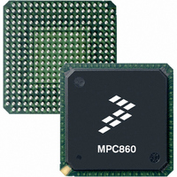
MC68MH360ZP33L Freescale Semiconductor, MC68MH360ZP33L Datasheet - Page 51

MC68MH360ZP33L
Manufacturer Part Number
MC68MH360ZP33L
Description
IC MPU 32BIT QUICC 357-PBGA
Manufacturer
Freescale Semiconductor
Specifications of MC68MH360ZP33L
Processor Type
M683xx 32-Bit
Speed
33MHz
Voltage
5V
Mounting Type
Surface Mount
Package / Case
357-PBGA
Lead Free Status / RoHS Status
Contains lead / RoHS non-compliant
Features
-
Available stocks
Company
Part Number
Manufacturer
Quantity
Price
Company:
Part Number:
MC68MH360ZP33L
Manufacturer:
FREESCALE
Quantity:
1 831
Company:
Part Number:
MC68MH360ZP33L
Manufacturer:
MOTOLOLA
Quantity:
672
Company:
Part Number:
MC68MH360ZP33L
Manufacturer:
Freescale Semiconductor
Quantity:
10 000
Part Number:
MC68MH360ZP33L
Manufacturer:
FREESCALE
Quantity:
20 000
Company:
Part Number:
MC68MH360ZP33LR2
Manufacturer:
Freescale Semiconductor
Quantity:
10 000
- Current page: 51 of 962
- Download datasheet (5Mb)
MOTOROLA
Bus Arbitration Bus Request
Bus Control
Controller
Address
Interrupt
Memory
Control
Group
Parity
Data
Address Bus
Address Bus/Byte
Write Enables
Function Codes
Data Bus 31–16
Data Bus 15–0
Parity 2–0
Parity3/16BM
Parity Error
Chip Select/Row Ad-
dress Select 7/
Interrupt Acknowl-
edge 7
Chip Select 6–0/
Row Address Select
6–0
Column Address Se-
lect 3–0/Interrupt Ac-
knowledge 1, 2, 3, 6
Bus Grant
Bus Grant Acknowl-
edge
Read-Modify-Write
Cycle/Initial Configu-
ration 0
Bus Clear Out/
Initial Configuration
1/Row Address Se-
lect 2 Double-Drive
Data and Size Ac-
knowledge
Address Strobe
Data Strobe
Size
Read/Write
Output Enable/
Address Multiplex
Interrupt Request
Level 7–1
Autovector/Interrupt
Table 2-1. System Bus Signal Index (Normal Operation)
Acknowledge 5
Signal Name
Freescale Semiconductor, Inc.
For More Information On This Product,
DSACK1–DSACK0
BCLRO/CONFIG1/
CS/RAS7/IACK7 Enables peripherals or DRAMs at programmed addresses
PRTY2–PRTY0
RMC/CONFIG0
PRTY3/16BM
AVEC/IACK5
RAS6–RAS0
CAS3-CAS0/
MC68360 USER’S MANUAL
IACK6,3,2,1
IRQ7–IRQ1
Go to: www.freescale.com
Mnemonic
WE0–WE3
SIZ1–SIZ0
CS6–CS0/
OE/AMUX
A31–A28/
FC3–FC0
D31–D16
RAS2DD
A27–A0
D15–D0
BGACK
PERR
R/W
BR
BG
DS
AS
Lower 27 bits of address bus. (I/O)
Upper four bits of address bus (I/O), or byte write enable sig-
nals (O) for accesses to external memory or peripherals.
Identifies the processor state and the address space of the
current bus cycle. (I/O)
Upper 16-bit data bus used to transfer byte or word data.
Used in 16-bit bus mode (I/O).
Lower 16-bit data bus used to transfer 3-byte or long-word
data (I/O). Not used in 16-bit bus mode.
Parity signals for byte writes/reads from/to external memory
module (I/O).
Parity signals for byte writes/reads from/to external memory
module or defines 16-bit bus mode. (I/O)
Indicates a parity error during a read cycle. (O)
(O) or interrupt level 7 acknowledge line (O).
Enables peripherals or DRAMs at programmed addresses.
(O)
DRAM column address select or interrupt level acknowledge
lines. (O)
Indicates that an external device requires bus mastership. (I)
Indicates that the current bus cycle is complete and the
QUICC has relinquished the bus. (O)
Indicates that an external device has assumed bus master-
ship. (I)
Identifies the bus cycle as part of an indivisible read-modify-
write operation (I/O) or initial QUICC configuration select (I).
Indicates that an internal device requires the external bus
(Open-Drain O) or initial QUICC configuration select (I) or
row address select 2 double-drive output (O).
Provides asynchronous data transfer acknowledgement and
dynamic bus sizing (open-drain I/O but driven high before
three-stated).
Indicates that a valid address is on the address bus. (I/O)
During a read cycle, DS indicates that an external device
should place valid data on the data bus. During a write cycle,
DS indicates that valid data is on the data bus. (I/O)
Indicates the number of bytes remaining to be transferred for
this cycle. (I/O)
Indicates the direction of data transfer on the bus. (I/O)
Active during a read cycle indicates that an external device
should place valid data on the data bus (O) or provides a
strobe for external address multiplexing in DRAM accesses
if internal multiplexing is not used (O).
Provides external interrupt requests to the CPU32+ at prior-
ity levels 7–1. (I)
Autovector request during an interrupt acknowledge cycle
(open-drain I/O) or interrupt level 5 acknowledge line (O).
Function
Signal Descriptions
2-3
Related parts for MC68MH360ZP33L
Image
Part Number
Description
Manufacturer
Datasheet
Request
R
Part Number:
Description:
Manufacturer:
Freescale Semiconductor, Inc
Datasheet:
Part Number:
Description:
Manufacturer:
Freescale Semiconductor, Inc
Datasheet:
Part Number:
Description:
Manufacturer:
Freescale Semiconductor, Inc
Datasheet:
Part Number:
Description:
Manufacturer:
Freescale Semiconductor, Inc
Datasheet:
Part Number:
Description:
Manufacturer:
Freescale Semiconductor, Inc
Datasheet:
Part Number:
Description:
Manufacturer:
Freescale Semiconductor, Inc
Datasheet:
Part Number:
Description:
Manufacturer:
Freescale Semiconductor, Inc
Datasheet:
Part Number:
Description:
Manufacturer:
Freescale Semiconductor, Inc
Datasheet:
Part Number:
Description:
Manufacturer:
Freescale Semiconductor, Inc
Datasheet:
Part Number:
Description:
Manufacturer:
Freescale Semiconductor, Inc
Datasheet:
Part Number:
Description:
Manufacturer:
Freescale Semiconductor, Inc
Datasheet:
Part Number:
Description:
Manufacturer:
Freescale Semiconductor, Inc
Datasheet:
Part Number:
Description:
Manufacturer:
Freescale Semiconductor, Inc
Datasheet:
Part Number:
Description:
Manufacturer:
Freescale Semiconductor, Inc
Datasheet:
Part Number:
Description:
Manufacturer:
Freescale Semiconductor, Inc
Datasheet:


