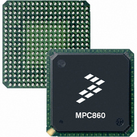
MC68MH360ZP33L Freescale Semiconductor, MC68MH360ZP33L Datasheet - Page 769

MC68MH360ZP33L
Manufacturer Part Number
MC68MH360ZP33L
Description
IC MPU 32BIT QUICC 357-PBGA
Manufacturer
Freescale Semiconductor
Specifications of MC68MH360ZP33L
Processor Type
M683xx 32-Bit
Speed
33MHz
Voltage
5V
Mounting Type
Surface Mount
Package / Case
357-PBGA
Lead Free Status / RoHS Status
Contains lead / RoHS non-compliant
Features
-
Available stocks
Company
Part Number
Manufacturer
Quantity
Price
Company:
Part Number:
MC68MH360ZP33L
Manufacturer:
FREESCALE
Quantity:
1 831
Company:
Part Number:
MC68MH360ZP33L
Manufacturer:
MOTOLOLA
Quantity:
672
Company:
Part Number:
MC68MH360ZP33L
Manufacturer:
Freescale Semiconductor
Quantity:
10 000
Part Number:
MC68MH360ZP33L
Manufacturer:
FREESCALE
Quantity:
20 000
Company:
Part Number:
MC68MH360ZP33LR2
Manufacturer:
Freescale Semiconductor
Quantity:
10 000
- Current page: 769 of 962
- Download datasheet (5Mb)
Applications
9.4.3.1 BASIC INITIALIZATION. The following paragraphs describe basic software initial-
ization.
The module base address register (MBAR) should be set as desired. However, the QUICC
8-Kbyte block of address space should not overlap any memory array.
The module base address register enable (MBARE) should not be accessed.
In the module configuration register (MCR), ASTM and BSTM should be set. The user
should program BCLROID2–BCLROID0 to $3 and program the SDMA, IDMA1, and IDMA2
arbitration IDs in the SDMA configuration register and IDMA channel configuration registers
to 4, 2, and 0, respectively, to allow the SDMA and DRAM refresh to preempt IDMA trans-
fers. SHEN1–SHEN0 should be left cleared. SUPV should be cleared. BCLRIID2–
BCLRIID0 are not used and can be programmed to $0. IARB3–IARB0 can be left pro-
grammed to $F to allow SIM interrupts to have priority over CPM interrupts that occur at the
same level.
In the system protection control register (SYPCR), DBFE should be cleared. BME should be
set. If the software watchdog is not used, the SWE bit should be cleared. If the software
watchdog is used, the SWRI bit should be left set to cause a system reset, rather than an
interrupt.
The periodic interrupt control register (PICR) may be set as desired.
The port E pin assignment register (PEPAR) should be set to $31C0, which configures three
IOUTx lines to go out on some of the IRQx pins, the RAS1DD pin, and the use of the WE
lines instead of the A31–A28 lines. It also configures the AMUX pin (assuming DRAM is
used in the system; otherwise, the OE function should be programmed), four CASx lines,
CS7, and AVECO.
9.4.3.2 CONFIGURING THE MEMORY CONTROLLER. The
describe configuring the memory controller registers.
The global memory register (GMR) should be configured as follows:
9-49
The RFCNT bits may be set as desired. At 25 MHz, an RFCNT value of 24 (decimal) gives
one refresh every 15.6 s.
RFEN should be set.
RCYC depends on the DRAM speed. At 25 MHz (an 80-ns DRAM SIMM), RCYC should
be 00.
PGS2–PGS0 is not relevant since page mode and internal address multiplexing is not
used.
DPS should be set to 00.
WBT40 depends on timing; it is usually cleared for 80-ns DRAM SIMMs.
WBTQ depends on timing; it is usually set for 80-ns DRAM SIMMs.
EMWS is not used in this design since there is only one QUICC. It should be cleared.
Freescale Semiconductor, Inc.
For More Information On This Product,
MC68360 USER’S MANUAL
Go to: www.freescale.com
following
paragraphs
MOTOROLA
Related parts for MC68MH360ZP33L
Image
Part Number
Description
Manufacturer
Datasheet
Request
R
Part Number:
Description:
Manufacturer:
Freescale Semiconductor, Inc
Datasheet:
Part Number:
Description:
Manufacturer:
Freescale Semiconductor, Inc
Datasheet:
Part Number:
Description:
Manufacturer:
Freescale Semiconductor, Inc
Datasheet:
Part Number:
Description:
Manufacturer:
Freescale Semiconductor, Inc
Datasheet:
Part Number:
Description:
Manufacturer:
Freescale Semiconductor, Inc
Datasheet:
Part Number:
Description:
Manufacturer:
Freescale Semiconductor, Inc
Datasheet:
Part Number:
Description:
Manufacturer:
Freescale Semiconductor, Inc
Datasheet:
Part Number:
Description:
Manufacturer:
Freescale Semiconductor, Inc
Datasheet:
Part Number:
Description:
Manufacturer:
Freescale Semiconductor, Inc
Datasheet:
Part Number:
Description:
Manufacturer:
Freescale Semiconductor, Inc
Datasheet:
Part Number:
Description:
Manufacturer:
Freescale Semiconductor, Inc
Datasheet:
Part Number:
Description:
Manufacturer:
Freescale Semiconductor, Inc
Datasheet:
Part Number:
Description:
Manufacturer:
Freescale Semiconductor, Inc
Datasheet:
Part Number:
Description:
Manufacturer:
Freescale Semiconductor, Inc
Datasheet:
Part Number:
Description:
Manufacturer:
Freescale Semiconductor, Inc
Datasheet:


