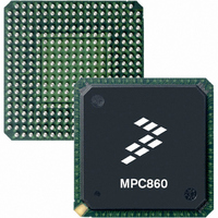
MC68MH360ZP33L Freescale Semiconductor, MC68MH360ZP33L Datasheet - Page 709

MC68MH360ZP33L
Manufacturer Part Number
MC68MH360ZP33L
Description
IC MPU 32BIT QUICC 357-PBGA
Manufacturer
Freescale Semiconductor
Specifications of MC68MH360ZP33L
Processor Type
M683xx 32-Bit
Speed
33MHz
Voltage
5V
Mounting Type
Surface Mount
Package / Case
357-PBGA
Lead Free Status / RoHS Status
Contains lead / RoHS non-compliant
Features
-
Available stocks
Company
Part Number
Manufacturer
Quantity
Price
Company:
Part Number:
MC68MH360ZP33L
Manufacturer:
FREESCALE
Quantity:
1 831
Company:
Part Number:
MC68MH360ZP33L
Manufacturer:
MOTOLOLA
Quantity:
672
Company:
Part Number:
MC68MH360ZP33L
Manufacturer:
Freescale Semiconductor
Quantity:
10 000
Part Number:
MC68MH360ZP33L
Manufacturer:
FREESCALE
Quantity:
20 000
Company:
Part Number:
MC68MH360ZP33LR2
Manufacturer:
Freescale Semiconductor
Quantity:
10 000
- Current page: 709 of 962
- Download datasheet (5Mb)
SECTION 8
SCAN CHAIN TEST ACCESS PORT
The QUICC provides a dedicated user-accessible test access port (TAP) that is JTAG com-
patible.
The QUICC TAP contains one additional signal not available with the MC68340 TAP—the
test reset (TRST) signal. This signal provides an asynchronous reset to the TAP.
The TAP consists of five dedicated signal pins, a 16-state TAP controller, and two test data
registers. A boundary scan register links all device signal pins into a single shift register. The
test logic, implemented utilizing static logic design, is independent of the device system log-
ic. The QUICC implementation provides the capability to:
In addition to the scan-test logic, the QUICC contains a signal that can be used to three-state
all QUICC output signals. This signal, called three-state (TRIS), is sampled during system
reset when the QUICC is not in slave mode.
8.1 OVERVIEW
An overview of the QUICC scan chain implementation is shown in Figure 8-1. The QUICC
implementation includes a TAP controller, a 3-bit instruction register, and two test registers
(a 1-bit bypass register and a 196-bit boundary scan register). This implementation includes
a dedicated TAP consisting of the following signals:
MOTOROLA
1. Perform boundary scan operations to test circuit-board electrical continuity.
2. Bypass the QUICC for a given circuit-board test by effectively reducing the boundary
3. Sample the QUICC system pins during operation and transparently shift out the result
4. Disable the output drive to pins during circuit-board testing.
• TCK—a test clock input to synchronize the test logic.
• TMS—a test mode select input (with an internal pullup resistor) that is sampled on the
• TDI—a test data input (with an internal pullup resistor) that is sampled on the rising
rising edge of TCK to sequence the TAP controller’s state machine.
edge of TCK.
scan register to a single cell.
in the boundary scan register.
Certain precautions must be observed to ensure that the IEEE
1149.-like test logic does not interfere with nontest operation.
See 8.6 Non-Scan Chain Operation for details.
Freescale Semiconductor, Inc.
For More Information On This Product,
MC68360 USER’S MANUAL
Go to: www.freescale.com
NOTE
8-1
Related parts for MC68MH360ZP33L
Image
Part Number
Description
Manufacturer
Datasheet
Request
R
Part Number:
Description:
Manufacturer:
Freescale Semiconductor, Inc
Datasheet:
Part Number:
Description:
Manufacturer:
Freescale Semiconductor, Inc
Datasheet:
Part Number:
Description:
Manufacturer:
Freescale Semiconductor, Inc
Datasheet:
Part Number:
Description:
Manufacturer:
Freescale Semiconductor, Inc
Datasheet:
Part Number:
Description:
Manufacturer:
Freescale Semiconductor, Inc
Datasheet:
Part Number:
Description:
Manufacturer:
Freescale Semiconductor, Inc
Datasheet:
Part Number:
Description:
Manufacturer:
Freescale Semiconductor, Inc
Datasheet:
Part Number:
Description:
Manufacturer:
Freescale Semiconductor, Inc
Datasheet:
Part Number:
Description:
Manufacturer:
Freescale Semiconductor, Inc
Datasheet:
Part Number:
Description:
Manufacturer:
Freescale Semiconductor, Inc
Datasheet:
Part Number:
Description:
Manufacturer:
Freescale Semiconductor, Inc
Datasheet:
Part Number:
Description:
Manufacturer:
Freescale Semiconductor, Inc
Datasheet:
Part Number:
Description:
Manufacturer:
Freescale Semiconductor, Inc
Datasheet:
Part Number:
Description:
Manufacturer:
Freescale Semiconductor, Inc
Datasheet:
Part Number:
Description:
Manufacturer:
Freescale Semiconductor, Inc
Datasheet:


