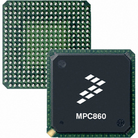
MC68MH360ZP33L Freescale Semiconductor, MC68MH360ZP33L Datasheet - Page 319

MC68MH360ZP33L
Manufacturer Part Number
MC68MH360ZP33L
Description
IC MPU 32BIT QUICC 357-PBGA
Manufacturer
Freescale Semiconductor
Specifications of MC68MH360ZP33L
Processor Type
M683xx 32-Bit
Speed
33MHz
Voltage
5V
Mounting Type
Surface Mount
Package / Case
357-PBGA
Lead Free Status / RoHS Status
Contains lead / RoHS non-compliant
Features
-
Available stocks
Company
Part Number
Manufacturer
Quantity
Price
Company:
Part Number:
MC68MH360ZP33L
Manufacturer:
FREESCALE
Quantity:
1 831
Company:
Part Number:
MC68MH360ZP33L
Manufacturer:
MOTOLOLA
Quantity:
672
Company:
Part Number:
MC68MH360ZP33L
Manufacturer:
Freescale Semiconductor
Quantity:
10 000
Part Number:
MC68MH360ZP33L
Manufacturer:
FREESCALE
Quantity:
20 000
Company:
Part Number:
MC68MH360ZP33LR2
Manufacturer:
Freescale Semiconductor
Quantity:
10 000
- Current page: 319 of 962
- Download datasheet (5Mb)
DSSEL—Dynamic RAM Select
SPS1–SPS0—SRAM Port Size (SRAM Bank Only)
PGME—Page Mode Enabled (DRAM Banks Only)
MOTOROLA
This bit determines if the bank is a DRAM or SRAM, which impacts a number of signals:
1) the length of the cycle is different; 2) address muxing is performed if GAMX = 1; and 3)
the previous RAS is negated if a page bank miss occurs and DSSEL = 1 (for the new
bank).
This attribute determines whether a given chip select responds with DSACKx and, if so,
what port size is returned (see Table 6-13).
If the cycle is terminated by using the internal wait-state attributes, the QUICC drives the
DSACKx lines according to those bits. If the internal wait-state attributes are not used, the
cycle should be terminated with external DSACKx. In this case, the QUICC does not drive
the DSACKx lines, but rather samples them at every falling edge of the clock.
If an MC68EC040 access is performed using this SRAM bank and SPS= 00, 01, or 10,
the SRAM controller operates in the same way, except it asserts TA instead of DSACKx.
If SPS= 11, TA is sampled at every rising edge of the clock.
This bit is used to enable page mode accesses to a DRAM bank. Page mode accesses
are performed only for an internal QUICC or an external QUICC/MC68030-type master.
0 = SRAM bank (i.e., SRAM, EPROM, peripherals, etc.)
1 = DRAM bank
0 = Page mode is disabled.
1 = Page mode is enabled.
If DSACK is provided internally, then the DSACKx lines are still
sampled externally, and can be asserted externally to end the
cycle. However, in this case of external DSACKx assertion, ex-
ternal DSACKx should be asserted and negated prior to when
internal DSACK would have been asserted by the QUICC. This
is easily accomplished on the boot chip select since the QUICC
default value is 14 wait states.
The SRAM controller does not support an external TA response
for MC68040 burst mode. Also, for non-burst MC68040 cycles,
TA cannot be externally asserted before CS is asserted.
Freescale Semiconductor, Inc.
For More Information On This Product,
SPS1–SPS0
Table 6-13. SRAM Port Size
00
01
10
11
MC68360 USER’S MANUAL
Go to: www.freescale.com
32-Bit Port Size
16-Bit Port Size
8-Bit Port Size
External DSACKx Response
NOTES
Result
System Integration Module (SIM60)
6-75
Related parts for MC68MH360ZP33L
Image
Part Number
Description
Manufacturer
Datasheet
Request
R
Part Number:
Description:
Manufacturer:
Freescale Semiconductor, Inc
Datasheet:
Part Number:
Description:
Manufacturer:
Freescale Semiconductor, Inc
Datasheet:
Part Number:
Description:
Manufacturer:
Freescale Semiconductor, Inc
Datasheet:
Part Number:
Description:
Manufacturer:
Freescale Semiconductor, Inc
Datasheet:
Part Number:
Description:
Manufacturer:
Freescale Semiconductor, Inc
Datasheet:
Part Number:
Description:
Manufacturer:
Freescale Semiconductor, Inc
Datasheet:
Part Number:
Description:
Manufacturer:
Freescale Semiconductor, Inc
Datasheet:
Part Number:
Description:
Manufacturer:
Freescale Semiconductor, Inc
Datasheet:
Part Number:
Description:
Manufacturer:
Freescale Semiconductor, Inc
Datasheet:
Part Number:
Description:
Manufacturer:
Freescale Semiconductor, Inc
Datasheet:
Part Number:
Description:
Manufacturer:
Freescale Semiconductor, Inc
Datasheet:
Part Number:
Description:
Manufacturer:
Freescale Semiconductor, Inc
Datasheet:
Part Number:
Description:
Manufacturer:
Freescale Semiconductor, Inc
Datasheet:
Part Number:
Description:
Manufacturer:
Freescale Semiconductor, Inc
Datasheet:
Part Number:
Description:
Manufacturer:
Freescale Semiconductor, Inc
Datasheet:


