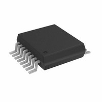
AD5933YRSZ Analog Devices Inc, AD5933YRSZ Datasheet - Page 28

AD5933YRSZ
Manufacturer Part Number
AD5933YRSZ
Description
IC NTWK ANALYZER 12B 1MSP 16SSOP
Manufacturer
Analog Devices Inc
Datasheet
1.AD5933YRSZ.pdf
(44 pages)
Specifications of AD5933YRSZ
Resolution (bits)
12 b
Master Fclk
16.776MHz
Voltage - Supply
2.7 V ~ 5.5 V
Operating Temperature
-40°C ~ 125°C
Mounting Type
Surface Mount
Package / Case
16-SSOP
Supply Voltage Range
2.7V To 5.5V
Operating Temperature Range
-40°C To +125°C
Digital Ic Case Style
SSOP
No. Of Pins
16
Frequency Max
0.1MHz
Termination Type
SMD
Pin Count
16
Screening Level
Automotive
Package Type
SSOP
Filter Terminals
SMD
Rohs Compliant
Yes
Communication Function
Network Analyzer
Lead Free Status / RoHS Status
Lead free / RoHS Compliant
For Use With
EVAL-AD5933EBZ - BOARD EVALUATION FOR AD5933
Tuning Word Width (bits)
-
Lead Free Status / Rohs Status
Compliant
Other names
AD5933BRSZ
Q2204656A
Q2204656A
Available stocks
Company
Part Number
Manufacturer
Quantity
Price
Company:
Part Number:
AD5933YRSZ
Manufacturer:
ADI
Quantity:
5 000
Company:
Part Number:
AD5933YRSZ
Manufacturer:
Fujitsu
Quantity:
500
Part Number:
AD5933YRSZ
Manufacturer:
ADI/亚德诺
Quantity:
20 000
AD5933
SERIAL BUS INTERFACE
Control of the AD5933 is carried out via the I
serial interface protocol. The AD5933 is connected to this bus
as a slave device under the control of a master device. The
AD5933 has a 7-bit serial bus slave address. When the device is
powered up, it has a default serial bus address, 0001101 (0x0D).
GENERAL I
Figure 35 shows the timing diagram for general read and write
operations using the I
The master initiates data transfer by establishing a start condition,
defined as a high-to-low transition on the serial data line
(SDA), while the serial clock line (SCL) remains high. This
indicates that a data stream follows. The slave responds to the
start condition and shifts in the next 8 bits, consisting of a 7-bit
slave address (MSB first) plus an R/W bit that determines
the direction of the data transfer—that is, whether data is
written to or read from the slave device (0 = write, 1 = read).
The slave responds by pulling the data line low during the low
period before the ninth clock pulse, known as the acknowledge
bit, and holding it low during the high period of this clock
pulse. All other devices on the bus remain idle while the
selected device waits for data to be read from or written to it.
If the R/W bit is 0, then the master writes to the slave device.
If the R/W bit is 1, the master reads from the slave device.
SDA
START CONDITION
BY MASTER
2
C TIMING
2
0
C-compliant interface.
0
SLAVE ADDRESS BYTE
0
1
1
2
C-compliant
0
1
Figure 35. Timing Diagram
ACKNOWLEDGE BY
R/W
Rev. C | Page 28 of 44
AD5933
D7
Data is sent over the serial bus in sequences of nine clock
pulses, eight bits of data followed by an acknowledge bit, which
can be from the master or slave device. Data transitions on the
data line must occur during the low period of the clock signal
and remain stable during the high period, because a low-to-
high transition when the clock is high may be interpreted as a
stop signal. If the operation is a write operation, the first data
byte after the slave address is a command byte. This tells the
slave device what to expect next. It may be an instruction telling
the slave device to expect a block write, or it may be a register
address that tells the slave where subsequent data is to be
written. Because data can flow in only one direction as defined
by the R/W bit, it is not possible to send a command to a slave
device during a read operation. Before performing a read
operation, it is sometimes necessary to perform a write
operation to tell the slave what sort of read operation to
expect and/or the address from which data is to be read.
When all data bytes have been read or written, stop conditions
are established. In write mode, the master pulls the data line
high during the 10
read mode, the master device releases the SDA line during the
low period before the ninth clock pulse, but the slave device
does not pull it low. This is known as a no acknowledge. The
master then takes the data line low during the low period
before the 10
pulse to assert a stop condition.
D6
D5
REGISTER ADDRESS
th
D4
clock pulse, then high during the 10
th
D3
clock pulse to assert a stop condition. In
D2
D1
D0
ACKNOWLEDGE BY
MASTER/SLAVE
th
clock


