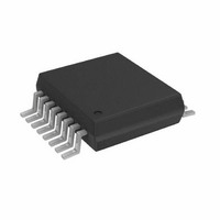
AD5933YRSZ Analog Devices Inc, AD5933YRSZ Datasheet - Page 4

AD5933YRSZ
Manufacturer Part Number
AD5933YRSZ
Description
IC NTWK ANALYZER 12B 1MSP 16SSOP
Manufacturer
Analog Devices Inc
Datasheet
1.AD5933YRSZ.pdf
(44 pages)
Specifications of AD5933YRSZ
Resolution (bits)
12 b
Master Fclk
16.776MHz
Voltage - Supply
2.7 V ~ 5.5 V
Operating Temperature
-40°C ~ 125°C
Mounting Type
Surface Mount
Package / Case
16-SSOP
Supply Voltage Range
2.7V To 5.5V
Operating Temperature Range
-40°C To +125°C
Digital Ic Case Style
SSOP
No. Of Pins
16
Frequency Max
0.1MHz
Termination Type
SMD
Pin Count
16
Screening Level
Automotive
Package Type
SSOP
Filter Terminals
SMD
Rohs Compliant
Yes
Communication Function
Network Analyzer
Lead Free Status / RoHS Status
Lead free / RoHS Compliant
For Use With
EVAL-AD5933EBZ - BOARD EVALUATION FOR AD5933
Tuning Word Width (bits)
-
Lead Free Status / Rohs Status
Compliant
Other names
AD5933BRSZ
Q2204656A
Q2204656A
Available stocks
Company
Part Number
Manufacturer
Quantity
Price
Company:
Part Number:
AD5933YRSZ
Manufacturer:
ADI
Quantity:
5 000
Company:
Part Number:
AD5933YRSZ
Manufacturer:
Fujitsu
Quantity:
500
Part Number:
AD5933YRSZ
Manufacturer:
ADI/亚德诺
Quantity:
20 000
AD5933
SPECIFICATIONS
VDD = 3.3 V, MCLK = 16.776 MHz, 2 V p-p output excitation voltage @ 30 kHz, 200 kΩ connected between Pin 5 and Pin 6; feedback
resistor = 200 kΩ connected between Pin 4 and Pin 5; PGA gain = ×1, unless otherwise noted.
Table 1.
Parameter
SYSTEM
TRANSMIT STAGE
TRANSMIT OUTPUT VOLTAGE
SYSTEM AC CHARACTERISTICS
Impedance Range
Total System Accuracy
System Impedance Error Drift
Output Frequency Range
Output Frequency Resolution
MCLK Frequency
Internal Oscillator Frequency
Internal Oscillator Temperature Coefficient
Range 1
Range 2
Range 3
Range 4
Signal-to-Noise Ratio
Total Harmonic Distortion
Spurious-Free Dynamic Range
Wide Band (0 MHz to 1 MHz)
Narrow Band (±5 kHz)
AC Output Excitation Voltage
DC Bias
DC Output Impedance
Short-Circuit Current to Ground at VOUT
AC Output Excitation Voltage
DC Bias
DC Output Impedance
Short-Circuit Current to Ground at VOUT
AC Output Excitation Voltage
DC Bias
DC Output Impedance
Short-Circuit Current to Ground at VOUT
AC Output Excitation Voltage
DC Bias
DC Output Impedance
Short-Circuit Current to Ground at VOUT
5
5
5
5
2
3
4
4
4
4
Min
1 K
1
Rev. C | Page 4 of 44
Y Version
Typ
0.5
30
0.1
16.776
30
1.98
1.48
200
±5.8
0.97
0.76
2.4
±0.25
0.383
0.31
1
±0.20
0.198
0.173
600
±0.15
60
−52
−56
−85
1
Max
10 M
100
16.776
Unit
Ω
%
ppm/°C
kHz
Hz
MHz
MHz
ppm/°C
V p-p
V
Ω
mA
V p-p
V
kΩ
mA
V p-p
V
kΩ
mA
V p-p
V
Ω
mA
dB
dB
dB
dB
DC bias of the ac excitation signal;
Test Conditions/Comments
100 Ω to 1 kΩ requires extra buffer
circuitry, see the Measuring Small
Impedances section
2 V p-p output excitation voltage at
30 kHz, 200 kΩ connected between
Pin 5 and Pin 6
<0.1 Hz resolution achievable using
DDS techniques
Maximum system clock frequency
Frequency of internal clock
See Figure 4 for output voltage
distribution
see Figure 5
T
T
See Figure 6
DC bias of output excitation signal;
see Figure 7
See Figure 8
DC bias of output excitation signal;
see Figure 9
See Figure 10
DC bias of output excitation signal.
See Figure 11
A
A
= 25°C
= 25°C


