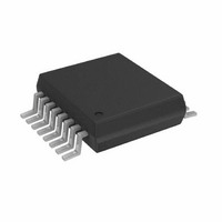
AD5933YRSZ Analog Devices Inc, AD5933YRSZ Datasheet - Page 5

AD5933YRSZ
Manufacturer Part Number
AD5933YRSZ
Description
IC NTWK ANALYZER 12B 1MSP 16SSOP
Manufacturer
Analog Devices Inc
Datasheet
1.AD5933YRSZ.pdf
(44 pages)
Specifications of AD5933YRSZ
Resolution (bits)
12 b
Master Fclk
16.776MHz
Voltage - Supply
2.7 V ~ 5.5 V
Operating Temperature
-40°C ~ 125°C
Mounting Type
Surface Mount
Package / Case
16-SSOP
Supply Voltage Range
2.7V To 5.5V
Operating Temperature Range
-40°C To +125°C
Digital Ic Case Style
SSOP
No. Of Pins
16
Frequency Max
0.1MHz
Termination Type
SMD
Pin Count
16
Screening Level
Automotive
Package Type
SSOP
Filter Terminals
SMD
Rohs Compliant
Yes
Communication Function
Network Analyzer
Lead Free Status / RoHS Status
Lead free / RoHS Compliant
For Use With
EVAL-AD5933EBZ - BOARD EVALUATION FOR AD5933
Tuning Word Width (bits)
-
Lead Free Status / Rohs Status
Compliant
Other names
AD5933BRSZ
Q2204656A
Q2204656A
Available stocks
Company
Part Number
Manufacturer
Quantity
Price
Company:
Part Number:
AD5933YRSZ
Manufacturer:
ADI
Quantity:
5 000
Company:
Part Number:
AD5933YRSZ
Manufacturer:
Fujitsu
Quantity:
500
Part Number:
AD5933YRSZ
Manufacturer:
ADI/亚德诺
Quantity:
20 000
Parameter
RECEIVE STAGE
ANALOG-TO-DIGITAL CONVERTER
TEMPERATURE SENSOR
LOGIC INPUTS
POWER REQUIREMENTS
1
2
3
4
5
6
7
Temperature range for Y version = −40°C to +125°C, typical at 25°C.
The lower limit of the output excitation frequency can be lowered by scaling the clock supplied to the AD5933.
Refer to Figure 14, Figure 15, and Figure 16 for the internal oscillator frequency distribution with temperature.
The peak-to-peak value of the ac output excitation voltage scales with supply voltage according to the following formula:
The dc bias value of the output excitation voltage scales with supply voltage according to the following formula:
Guaranteed by design or characterization, not production tested. Input capacitance at the VOUT pin is equal to pin capacitance divided by open-loop gain of current-
to-voltage amplifier.
The accumulation of the currents into Pin 8, Pin 15, and Pin 16.
Input Leakage Current
Input Capacitance
Feedback Capacitance (C
Resolution
Sampling Rate
Accuracy
Resolution
Temperature Conversion Time
Input High Voltage (V
Input Low Voltage (V
Input Current
Input Capacitance
VDD
IDD (Normal Mode )
IDD (Standby Mode)
IDD (Power-Down Mode)
Output Excitation Voltage (V p-p) = [2/3.3] × VDD
where VDD is the supply voltage.
Output Excitation Bias Voltage (V) = [2/3.3] × VDD
where VDD is the supply voltage.
7
6
IL
IH
)
)
FB
)
6
Min
0.7 × VDD
2.7
Rev. C | Page 5 of 44
Y Version
Typ
1
0.01
3
12
250
±2.0
0.03
800
10
17
11
16
0.7
1
1
Max
0.3 × VDD
1
7
5.5
15
25
5
8
Unit
nA
pF
pF
Bits
kSPS
°C
°C
μs
μA
pF
V
mA
mA
mA
mA
μA
μA
VDD = 3.3 V
Test Conditions/Comments
To VIN pin
Pin capacitance between VIN and GND
Feedback capacitance around current-
to-voltage amplifier; appears in
parallel with feedback resistor
ADC throughput rate
−40°C to +125°C temperature range
Conversion time of single temperature
measurement
T
T
VDD = 5.5 V
VDD = 3.3 V; see the Control Register
(Register Address 0X80, Register
Address 0X81) section
VDD = 5.5 V
VDD = 3.3 V
VDD = 5.5 V
A
A
= 25°C
= 25°C
AD5933


