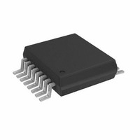
AD5933YRSZ Analog Devices Inc, AD5933YRSZ Datasheet - Page 6

AD5933YRSZ
Manufacturer Part Number
AD5933YRSZ
Description
IC NTWK ANALYZER 12B 1MSP 16SSOP
Manufacturer
Analog Devices Inc
Datasheet
1.AD5933YRSZ.pdf
(44 pages)
Specifications of AD5933YRSZ
Resolution (bits)
12 b
Master Fclk
16.776MHz
Voltage - Supply
2.7 V ~ 5.5 V
Operating Temperature
-40°C ~ 125°C
Mounting Type
Surface Mount
Package / Case
16-SSOP
Supply Voltage Range
2.7V To 5.5V
Operating Temperature Range
-40°C To +125°C
Digital Ic Case Style
SSOP
No. Of Pins
16
Frequency Max
0.1MHz
Termination Type
SMD
Pin Count
16
Screening Level
Automotive
Package Type
SSOP
Filter Terminals
SMD
Rohs Compliant
Yes
Communication Function
Network Analyzer
Lead Free Status / RoHS Status
Lead free / RoHS Compliant
For Use With
EVAL-AD5933EBZ - BOARD EVALUATION FOR AD5933
Tuning Word Width (bits)
-
Lead Free Status / Rohs Status
Compliant
Other names
AD5933BRSZ
Q2204656A
Q2204656A
Available stocks
Company
Part Number
Manufacturer
Quantity
Price
Company:
Part Number:
AD5933YRSZ
Manufacturer:
ADI
Quantity:
5 000
Company:
Part Number:
AD5933YRSZ
Manufacturer:
Fujitsu
Quantity:
500
Part Number:
AD5933YRSZ
Manufacturer:
ADI/亚德诺
Quantity:
20 000
AD5933
I
VDD = 2.7 V to 5.5 V. All specifications T
Table 2.
Parameter
f
t
t
t
t
t
t
t
t
t
t
t
C
1
2
3
4
SCL
1
2
3
4
5
6
7
8
9
10
11
2
See Figure 2.
Guaranteed by design and characterization, not production tested.
A master device must provide a hold time of at least 300 ns for the SDA signal (referred to V
C
b
3
C SERIAL INTERFACE TIMING CHARACTERISTICS
b
is the total capacitance of one bus line in picofarads. Note that t
2
SDA
SCL
Limit at T
400
2.5
0.6
1.3
0.6
100
0.9
0
0.6
0.6
1.3
300
0
300
0
250
20 + 0.1 C
400
t
9
CONDITION
MIN
b
4
START
, T
t
4
MAX
t
3
MIN
to T
Unit
kHz max
μs min
μs min
μs min
μs min
ns min
μs max
μs min
μs min
μs min
μs min
ns max
ns min
ns max
ns min
ns max
ns min
pF max
MAX
t
10
t
6
, unless otherwise noted.
Figure 2. I
t
R
11
and t
t
2
Rev. C | Page 6 of 44
F
2
Description
SCL clock frequency
SCL cycle time
t
t
t
t
t
t
t
t
t
t
t
t
t
t
t
Capacitive load for each bus line
C Interface Timing Diagram
are measured between 0.3 VDD and 0.7 VDD.
HIGH
LOW
HD, STA
SU, DAT
HD, DAT
HD, DAT
SU, STA
SU, STO
BUF
F
R
F
F
F
F
, rise time of SDA when transmitting
, fall time of SCL and SDA when transmitting
, fall time of SDA when receiving (CMOS compatible)
, fall time of SDA when receiving
, fall time of SCL and SDA when transmitting
, rise time of SCL and SDA when receiving (CMOS compatible)
, bus free time between a stop and a start condition
, SCL low time
, SCL high time
, setup time for repeated start
, stop condition setup time
, start/repeated start condition hold time
, data setup time
, data hold time
, data hold time
t
5
IH MIN
1
t
7
CONDITION
REPEATED
of the SCL signal) to bridge the undefined falling edge of SCL.
START
t
4
t
1
CONDITION
STOP
t
8


