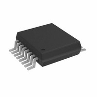
AD5933YRSZ Analog Devices Inc, AD5933YRSZ Datasheet - Page 31

AD5933YRSZ
Manufacturer Part Number
AD5933YRSZ
Description
IC NTWK ANALYZER 12B 1MSP 16SSOP
Manufacturer
Analog Devices Inc
Datasheet
1.AD5933YRSZ.pdf
(44 pages)
Specifications of AD5933YRSZ
Resolution (bits)
12 b
Master Fclk
16.776MHz
Voltage - Supply
2.7 V ~ 5.5 V
Operating Temperature
-40°C ~ 125°C
Mounting Type
Surface Mount
Package / Case
16-SSOP
Supply Voltage Range
2.7V To 5.5V
Operating Temperature Range
-40°C To +125°C
Digital Ic Case Style
SSOP
No. Of Pins
16
Frequency Max
0.1MHz
Termination Type
SMD
Pin Count
16
Screening Level
Automotive
Package Type
SSOP
Filter Terminals
SMD
Rohs Compliant
Yes
Communication Function
Network Analyzer
Lead Free Status / RoHS Status
Lead free / RoHS Compliant
For Use With
EVAL-AD5933EBZ - BOARD EVALUATION FOR AD5933
Tuning Word Width (bits)
-
Lead Free Status / Rohs Status
Compliant
Other names
AD5933BRSZ
Q2204656A
Q2204656A
Available stocks
Company
Part Number
Manufacturer
Quantity
Price
Company:
Part Number:
AD5933YRSZ
Manufacturer:
ADI
Quantity:
5 000
Company:
Part Number:
AD5933YRSZ
Manufacturer:
Fujitsu
Quantity:
500
Part Number:
AD5933YRSZ
Manufacturer:
ADI/亚德诺
Quantity:
20 000
TYPICAL APPLICATIONS
MEASURING SMALL IMPEDANCES
The AD5933 is capable of measuring impedance values up to
10 MΩ if the system gain settings are chosen correctly for the
impedance subrange of interest.
If the user places a small impedance value (≤500 Ω over the
sweep frequency of interest) between the VOUT and VIN pins,
it results in an increase in signal current flowing through the
impedance for a fixed excitation voltage in accordance with
Ohm’s law. The output stage of the transmit side amplifier
available at the VOUT pin may not be able to provide the
required increase in current through the impedance. To have a
unity gain condition about the receive side I-V amplifier, the
user needs to have a similar small value of feedback resistance
for system calibration as outlined in the Gain Factor Setup
Configuration section. The voltage presented at the VIN pin is
hard biased at VDD/2 due to the virtual earth on the receive
side I-V amplifier. The increased current sink/source
requirement placed on the output of the receive side I-V
amplifier may also cause the amplifier to operate outside of
the linear region. This causes significant errors in subsequent
impedance measurements.
The value of the output series resistance, R
at the VOUT pin must be taken into account when measuring
small impedances (Z
the output series resistance is comparable to the value of the
impedance under test (Z
counted for in the system calibration (that is, the gain factor
calculation) when measuring small impedances, there is an
introduced error into any subsequent impedance measurement
that takes place. The introduced error depends on the relative
magnitude of the impedance being tested compared to the value
of the output series resistance.
Figure 41. Additional External Amplifier Circuit for Measuring Small
DDS
OUTPUT AMPLIFIER
TRANSMIT SIDE
PGA
UNKNOWN
R
OUT
I-V
UNKNOWN
VDD/2
Impedances
VOUT
RFB
VIN
), specifically when the value of
2V p-p
). If the R
R
20kΩ
20kΩ
FB
V
DD
Z
R2
UNKNOWN
OUT
VDD/2
1µF
OUT
value is unac-
, (see Figure 41)
R1
AD8531
AD820
AD8641
AD8627
Rev. C | Page 31 of 44
The value of the output series resistance depends upon the
selected output excitation range at VOUT and has a tolerance
from device to device like all discrete resistors manufactured in
a silicon fabrication process. Typical values of the output series
resistance are outlined in Table 17.
Table 17. Output Series Resistance (R
Parameter
Range 1
Range 2
Range 3
Range 4
Therefore, to accurately calibrate the AD5933 to measure small
impedances, it is necessary to reduce the signal current by
attenuating the excitation voltage sufficiently and also account
for the R
(see the Gain Factor Calculation section).
Measuring the R
achieved by selecting the appropriate output excitation range at
VOUT and sinking and sourcing a known current at the pin
(for example, ±2 mA) and measuring the change in dc voltage.
The output series resistance can be calculated by measuring the
inverse of the slope (that is, 1/slope) of the resultant I-V plot.
A circuit that helps to minimize the effects of the issues
previously outlined is shown in Figure 41. The aim of this
circuit is to place the AD5933 system gain within its linear
range when measuring small impedances by using an additional
external amplifier circuit along the signal path. The external
amplifier attenuates the peak-to-peak excitation voltage at
VOUT by a suitable choice of resistors (R1 and R2), thereby
reducing the signal current flowing through the impedance and
minimizing the effect of the output series resistance in the
impedance calculations.
In the circuit shown in Figure 41, Z
output series resistance of the external amplifier which is
typically much less than 1 Ω with feedback applied depending
upon the op amp device used (for example, AD820, AD8641,
AD8531) as well as the load current, bandwidth, and gain.
OUT
value and factor it into the gain factor calculation
Value (Typ)
2 V p-p
1 V p-p
0.4 V p-p
0.2 V p-p
OUT
value during device characterization is
Output Series Resistance Value
200 Ω typ
2.4 kΩ typ
1.0 kΩ typ
600 Ω typ
UNKNOWN
OUT
) vs. Excitation Range
recognizes the
AD5933


