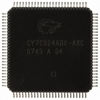
CY7C924ADX-AXC Cypress Semiconductor Corp, CY7C924ADX-AXC Datasheet - Page 27

CY7C924ADX-AXC
Manufacturer Part Number
CY7C924ADX-AXC
Description
IC TXRX HOTLINK 100LQFP
Manufacturer
Cypress Semiconductor Corp
Series
HOTlink™r
Type
Transceiverr
Specifications of CY7C924ADX-AXC
Package / Case
100-LQFP
Protocol
Fibre Channel
Voltage - Supply
4.5 V ~ 5.5 V
Mounting Type
Surface Mount
Product
Framer
Number Of Transceivers
1
Data Rate
622 Mbps
Supply Voltage (max)
5.5 V
Supply Voltage (min)
4.5 V
Supply Current (max)
250 mA
Maximum Operating Temperature
+ 70 C
Minimum Operating Temperature
0 C
Mounting Style
SMD/SMT
Operating Supply Voltage (typ)
5V
Screening Level
Commercial
Pin Count
100
Mounting
Surface Mount
Package Type
TQFP
Operating Supply Voltage (min)
4.5V
Operating Supply Voltage (max)
5.5V
Operating Temperature (min)
0C
Operating Temperature (max)
70C
Ic Interface Type
Parallel, Serial
Supply Voltage Range
4.5V To 5.5V
Operating Temperature Range
0°C To +70°C
Digital Ic Case Style
TQFP
No. Of Pins
100
No. Of Receivers
2
Frequency Max
50MHz
Rohs Compliant
Yes
Termination Type
SMD
Filter Terminals
SMD
Driver Case Style
TQFP
Lead Free Status / RoHS Status
Lead free / RoHS Compliant
Number Of Drivers/receivers
-
Lead Free Status / Rohs Status
Compliant
Other names
428-2918
CY7C924ADX-AXC
CY7C924ADX-AXC
Available stocks
Company
Part Number
Manufacturer
Quantity
Price
Company:
Part Number:
CY7C924ADX-AXC
Manufacturer:
CY
Quantity:
6
Company:
Part Number:
CY7C924ADX-AXC
Manufacturer:
CYPRESS
Quantity:
455
Company:
Part Number:
CY7C924ADX-AXC
Manufacturer:
Cypress Semiconductor Corp
Quantity:
10 000
Document #: 38-02008 Rev. *E
Capacitance
AC Test Loads and Waveforms
CY7C924ADX Transmitter TTL Switching Characteristics, FIFO Enabled
C
C
f
t
t
t
t
t
t
t
t
t
t
t
t
t
t
t
t
t
Notes
TS
TXCLK
TXCPWH
TXCPWL
TXCLKR
TXCLKF
TXA
TXDS
TXDH
TXENS
TXENH
TXRSS
TXRSH
TXAMS
TXAMH
TXZA
TXOE
TXAZ
8. Tested initially and after any design or process changes that may affect these parameters, but not 100% tested.
9. Cypress uses constant current (ATE) load configurations and forcing functions. This figure is for reference only.
10. Input/output rise and fall time is measured between 0.8V and 2.0V.
INTTL
INPECL
Parameter
Parameter
0.0V
3.0V
R1 = 500Ω
R2 = 333Ω
C
(Includes fixture and
probe capacitance)
L
[8]
V
[8]
≤ 1 ns
≤ 10 pF
th
=1.5V
[8]
TXCLK Clock Cycle Frequency With Transmit FIFO Enabled
TXCLK Period
TXCLK HIGH Time
TXCLK LOW Time
TXCLK Rise Time
TXCLK Fall Time
Flag Access Time From TXCLK↑ to Output
Transmit Data Setup Time to TXCLK↑
Transmit Data Hold Time from TXCLK↑
Transmit Enable Set-Up Time to TXCLK↑
Transmit Enable Hold Time from TXCLK↑
Transmit FIFO Reset (TXRST*) Setup Time to TXCLK↑
Transmit FIFO Reset (TXRST*) Hold Time from TXCLK↑
Transmit Address Match (AM*) Setup Time to TXCLK↑
Transmit Address Match (AM*) Hold Time from TXCLK↑
Sample of AM* LOW by TXCLK↑, Output High-Z to Active HIGH or LOW
Sample of AM* LOW by TXCLK↑ to Output Valid
Sample of AM* HIGH by TXCLK↑ to Output in High-Z
(c) TTL Input Test Waveform
TTL Input Capacitance
PECL-compatible input Capacitance
OUTPUT
2.0V
0.8V
(a) TTL AC Test Load
3.0V
Description
C
[10]
L
[10]
0.8V
2.0V
5.0V
Description
R1
R2
Note 9
V
th
≤ 1 ns
=1.5V
[9]
T
T
A
A
= 25°C, f
= 25°C, f
V
V
IHE
ILE
≤ 1 ns
(b) PECL AC Test Load
C
Test Conditions
0
0
L
= 1 MHz, V
= 1 MHz, V
20%
(d) PECL Input Test Waveform
DD
DD
80%
R
L
= 5.0V
= 5.0V
V
V
V
DD
[9]
IHE
Over the Operating Range
ILE
– 1.33V
Min
6.5
6.5
0.7
0.7
1.5
1.5
20
0
2
4
1
4
1
4
1
4
1
80%
R
C
(Includes fixture and
probe capacitance)
CY7C924ADX
L
L
= 50 Ω
< 5 pF
Max
7
4
20%
Max
≤ 1 ns
50
15
20
20
5
5
Page 27 of 58
Unit
pF
pF
MHz
Unit
ns
ns
ns
ns
ns
ns
ns
ns
ns
ns
ns
ns
ns
ns
ns
ns
ns
[+] Feedback


