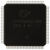
CY7C924ADX-AXC Cypress Semiconductor Corp, CY7C924ADX-AXC Datasheet - Page 35

CY7C924ADX-AXC
Manufacturer Part Number
CY7C924ADX-AXC
Description
IC TXRX HOTLINK 100LQFP
Manufacturer
Cypress Semiconductor Corp
Series
HOTlink™r
Type
Transceiverr
Specifications of CY7C924ADX-AXC
Package / Case
100-LQFP
Protocol
Fibre Channel
Voltage - Supply
4.5 V ~ 5.5 V
Mounting Type
Surface Mount
Product
Framer
Number Of Transceivers
1
Data Rate
622 Mbps
Supply Voltage (max)
5.5 V
Supply Voltage (min)
4.5 V
Supply Current (max)
250 mA
Maximum Operating Temperature
+ 70 C
Minimum Operating Temperature
0 C
Mounting Style
SMD/SMT
Operating Supply Voltage (typ)
5V
Screening Level
Commercial
Pin Count
100
Mounting
Surface Mount
Package Type
TQFP
Operating Supply Voltage (min)
4.5V
Operating Supply Voltage (max)
5.5V
Operating Temperature (min)
0C
Operating Temperature (max)
70C
Ic Interface Type
Parallel, Serial
Supply Voltage Range
4.5V To 5.5V
Operating Temperature Range
0°C To +70°C
Digital Ic Case Style
TQFP
No. Of Pins
100
No. Of Receivers
2
Frequency Max
50MHz
Rohs Compliant
Yes
Termination Type
SMD
Filter Terminals
SMD
Driver Case Style
TQFP
Lead Free Status / RoHS Status
Lead free / RoHS Compliant
Number Of Drivers/receivers
-
Lead Free Status / Rohs Status
Compliant
Other names
428-2918
CY7C924ADX-AXC
CY7C924ADX-AXC
Available stocks
Company
Part Number
Manufacturer
Quantity
Price
Company:
Part Number:
CY7C924ADX-AXC
Manufacturer:
CY
Quantity:
6
Company:
Part Number:
CY7C924ADX-AXC
Manufacturer:
CYPRESS
Quantity:
455
Company:
Part Number:
CY7C924ADX-AXC
Manufacturer:
Cypress Semiconductor Corp
Quantity:
10 000
Document #: 38-02008 Rev. *E
CY7C924ADX HOTLink Receiver Switching Waveforms
CY7C924ADX HOTLink Transceiver Operation
The interconnection of two or more CY7C924ADX Trans-
ceivers form a general-purpose communications subsystem
capable of transporting user data at up to 20 MBytes per
second over several types of serial interface media. The
CY7C924ADX is highly configurable with multiple modes of
operation.
In the transmit section of the CY7C924ADX, data moves from
the input register, through the Transmit FIFO, to the 8B/10B
Encoder. The encoded data is then shifted serially out the
OUTx± differential PECL-compatible drivers. The bit-rate
clock is generated internally from a 2.5x, 5x, or 10x PLL clock
multiplier (3x, 6x, or 12x if BYTE8/10* and ENCBYP* are
LOW). A more complete description is found in the section
CY7C924ADX HOTLink Transmit-Path Operating Mode
Description.
In the receive section of the CY7C924ADX, serial data is
sampled by the receiver on one of the INx± differential line
receiver inputs. The receiver clock and data recovery PLL
locks onto the selected serial bit stream and generates an
internal bit-rate sample clock. The bit stream is deserialized,
decoded, and presented to the Receive FIFO, along with a
character clock. The data in the FIFO can then be read either
slower or faster than the incoming character rate. A more
complete description is found in the section CY7C924ADX
HOTLink Receive-Path Operating Mode Description.
The Transmitter and Receiver parallel interface timing and
functionality can be configured to Cascade directly to external
FIFOs for depth expansion, to emulate a UTOPIA interface,
couple directly to registers, or couple directly to state
machines. These interfaces can accept or output either:
• 8-bit characters
• 10-bit characters (for byte-packed encoded transport)
• 10-bit pre-encoded characters (pre-scrambled or
• 12-bit pre-encoded characters (pre-scrambled or
pre-encoded)
pre-encoded)
REFCLK
Static Alignment
INA
INB
±
±
t
B
/2 – t
SAMPLE WINDOW
SA
t
REFL
t
B
/2 – t
SA
t
REFH
Error-Free Window
The bit numbering and content of the parallel transmit interface
is shown in
8B/10B Encoder bypassed, the TXSC/D* and RXSC/D* bits
are ignored.
The HOTLink Transceiver serial interface provides a seamless
interface to various types of media. A minimal number of
external passive components are required to properly
terminate transmission lines and provide LVPECL loads. For
power supply decoupling, a single capacitor (in the range of
0.02 μF to 0.1 μF) is required per power/ground pair. Additional
information on interfacing these components to various media
can be found in the HOTLink Design Considerations appli-
cation note.
CY7C924ADX HOTLink Transmit-Path
Operating Mode Description
The HOTLink Transmitter can be configured into several
operating modes, each providing different capabilities and
fitting different transmission needs. These modes are selected
using the FIFOBYP*, ENCBYP* and BYTE8/10* inputs on the
CY7C924ADX Transceiver. These modes can be reduced to
five primary classes:
Synchronous Encoded
In this mode, the Transmit FIFO is bypassed, while the 8B/10B
encoder is enabled. One character is accepted at the Transmit
Input Register at the rising edge of REFCLK, and passed to
the Encoder where it is encoded for serial transmission. The
Serializer operates synchronous to REFCLK, which is multi-
plied by 10 or 5 to generate the serial data bit-clock. In this
mode the TXSOC, TXRST*, TXINT, TXHALT*, and TXSTOP*
inputs (when they are not used for data bits) are not interpreted
• Synchronous Encoded
• Synchronous Pre-encoded
• Asynchronous Encoded
• Asynchronous Byte-packed
• Asynchronous Pre-encoded
INA
INB
(continued)
±
±
t
REFCLK
Table 1 on page
BIT CENTER
t
EFW
t
B
13. When operated with the
BIT CENTER
CY7C924ADX
Page 35 of 58
[+] Feedback


