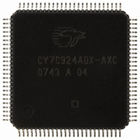
CY7C924ADX-AXC Cypress Semiconductor Corp, CY7C924ADX-AXC Datasheet - Page 44

CY7C924ADX-AXC
Manufacturer Part Number
CY7C924ADX-AXC
Description
IC TXRX HOTLINK 100LQFP
Manufacturer
Cypress Semiconductor Corp
Series
HOTlink™r
Type
Transceiverr
Specifications of CY7C924ADX-AXC
Package / Case
100-LQFP
Protocol
Fibre Channel
Voltage - Supply
4.5 V ~ 5.5 V
Mounting Type
Surface Mount
Product
Framer
Number Of Transceivers
1
Data Rate
622 Mbps
Supply Voltage (max)
5.5 V
Supply Voltage (min)
4.5 V
Supply Current (max)
250 mA
Maximum Operating Temperature
+ 70 C
Minimum Operating Temperature
0 C
Mounting Style
SMD/SMT
Operating Supply Voltage (typ)
5V
Screening Level
Commercial
Pin Count
100
Mounting
Surface Mount
Package Type
TQFP
Operating Supply Voltage (min)
4.5V
Operating Supply Voltage (max)
5.5V
Operating Temperature (min)
0C
Operating Temperature (max)
70C
Ic Interface Type
Parallel, Serial
Supply Voltage Range
4.5V To 5.5V
Operating Temperature Range
0°C To +70°C
Digital Ic Case Style
TQFP
No. Of Pins
100
No. Of Receivers
2
Frequency Max
50MHz
Rohs Compliant
Yes
Termination Type
SMD
Filter Terminals
SMD
Driver Case Style
TQFP
Lead Free Status / RoHS Status
Lead free / RoHS Compliant
Number Of Drivers/receivers
-
Lead Free Status / Rohs Status
Compliant
Other names
428-2918
CY7C924ADX-AXC
CY7C924ADX-AXC
Available stocks
Company
Part Number
Manufacturer
Quantity
Price
Company:
Part Number:
CY7C924ADX-AXC
Manufacturer:
CY
Quantity:
6
Company:
Part Number:
CY7C924ADX-AXC
Manufacturer:
CYPRESS
Quantity:
455
Company:
Part Number:
CY7C924ADX-AXC
Manufacturer:
Cypress Semiconductor Corp
Quantity:
10 000
Document #: 38-02008 Rev. *E
Synchronous With UTOPIA Timing and Control
(Transmit FIFO Bypassed)
When the Transmit FIFO is bypassed (FIFOBYP* is LOW and
not in byte-packed mode), the CY7C924ADX must still be
selected to write data into the Transmit Input Register.
Parallel TXDATA is clocked in and transmitted serially when
TXEN* is asserted. When TXEN* is deasserted, the TXDATA
bus contents are ignored and C5.0 idle characters are sent
instead.
AM* must be asserted to enable the TXFIFO flags. When AM*
is deasserted, the flags are High-Z.
When AM* is deasserted while TXEN* is enabled, the Transmit
TXDATA is still read in and transmitted, but the FIFO flags are
no longer enabled.
When data is not written to the Transmit Input Register, the
data stream is automatically padded with C5.0 (K28.5) SYNC
characters. If the 8B/10B Encoder is enabled, disparity
tracking allows the added C5.0 fill characters to follow all
8B/10B encoding rules. If the 8B/10B encoder is bypassed,
disparity tracking is disabled, and the transition between exter-
nally encoded data and internally generated C5.0 characters
may generate a running disparity error at the attached
receiver. The same error may occur at the transition between
the internal C5.0 characters and the resumption of externally
encoded data. When strings of contiguous C5.0 characters are
generated, each C5.0 has alternating running disparity with
the previous C5.0 character.
Receive Data Selection
Asynchronous With UTOPIA Timing and Control
(Receive FIFO Enabled)
When AM* is sampled LOW and RXRST* is sampled HIGH by
the rising edge of RXCLK input, an Rx_Match condition is
Rx_Selected
RXEMPTY
Rx_Match
RXDATA
RXRST*
RXCLK
RXEN
AM*
[26]
[26]
Figure 10. Receive Selection with Receive FIFO Enabled
Note 27
Not Empty
Note 27
Not Empty
generated. This Rx_Match condition continues until AM* is
sampled HIGH or RXRST* is sampled LOW at the rising edge
of RXCLK input. When an Rx_Match (or Rx_RstMatch)
condition is present, the RXEMPTY* and RXFULL* output
drivers are enabled. When an Rx_Match (or Rx_RstMatch)
condition is not present, these same drivers are disabled
(High-Z).
The selection state of the Receive FIFO is entered when an
Rx_Match condition is present, and RXEN* transitions from
HIGH to LOW. Once selected, the Receive FIFO remains
selected until RXEN* is sampled HIGH by the rising edge of
RXCLK input. The selected state initiates a read cycle from the
Receive FIFO and enables the Receive FIFO data onto the
RXDATA bus. This receive interface selection process is
shown in
RX_Match condition is not present when RXEN* is asserted
so the Receiver is not selected. However, the second RXEN*
assertion occurs with an RX_Match condition present and the
Receiver selection is successful.
Synchronous With UTOPIA Timing and Control
(Receive FIFO Bypassed)
When the Receive FIFO is bypassed (FIFOBYP* is LOW and
not in a byte-packed mode), the CY7C924ADX must still be
selected to enable the output drivers for the RXDATA bus. With
the Receive FIFO bypassed, RXCLK becomes a synchronous
output clock operating at the character rate.
The Receive interface is selected when AM* is sampled
asserted and RXEN* is asserted at least one cycle later. Once
selected, it remains asserted until RXEN* is deasserted,
regardless of the state of AM*.
D1
Figure
D2
10. For the first RXEN* assertion, the
D3
CY7C924ADX
Page 44 of 58
[+] Feedback


