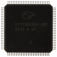
CY7C924ADX-AXC Cypress Semiconductor Corp, CY7C924ADX-AXC Datasheet - Page 8

CY7C924ADX-AXC
Manufacturer Part Number
CY7C924ADX-AXC
Description
IC TXRX HOTLINK 100LQFP
Manufacturer
Cypress Semiconductor Corp
Series
HOTlink™r
Type
Transceiverr
Specifications of CY7C924ADX-AXC
Package / Case
100-LQFP
Protocol
Fibre Channel
Voltage - Supply
4.5 V ~ 5.5 V
Mounting Type
Surface Mount
Product
Framer
Number Of Transceivers
1
Data Rate
622 Mbps
Supply Voltage (max)
5.5 V
Supply Voltage (min)
4.5 V
Supply Current (max)
250 mA
Maximum Operating Temperature
+ 70 C
Minimum Operating Temperature
0 C
Mounting Style
SMD/SMT
Operating Supply Voltage (typ)
5V
Screening Level
Commercial
Pin Count
100
Mounting
Surface Mount
Package Type
TQFP
Operating Supply Voltage (min)
4.5V
Operating Supply Voltage (max)
5.5V
Operating Temperature (min)
0C
Operating Temperature (max)
70C
Ic Interface Type
Parallel, Serial
Supply Voltage Range
4.5V To 5.5V
Operating Temperature Range
0°C To +70°C
Digital Ic Case Style
TQFP
No. Of Pins
100
No. Of Receivers
2
Frequency Max
50MHz
Rohs Compliant
Yes
Termination Type
SMD
Filter Terminals
SMD
Driver Case Style
TQFP
Lead Free Status / RoHS Status
Lead free / RoHS Compliant
Number Of Drivers/receivers
-
Lead Free Status / Rohs Status
Compliant
Other names
428-2918
CY7C924ADX-AXC
CY7C924ADX-AXC
Available stocks
Company
Part Number
Manufacturer
Quantity
Price
Company:
Part Number:
CY7C924ADX-AXC
Manufacturer:
CY
Quantity:
6
Company:
Part Number:
CY7C924ADX-AXC
Manufacturer:
CYPRESS
Quantity:
455
Company:
Part Number:
CY7C924ADX-AXC
Manufacturer:
Cypress Semiconductor Corp
Quantity:
10 000
Document #: 38-02008 Rev. *E
Pin Descriptions
CY7C924ADX HOTLink Transceiver
69
8
10
19
Number
Pin
RXEN*
RXCLK
RXFULL*
RXHALF*
Name
(continued)
TTL input, sampled
on RXCLK↑,
Internal Pull Up
Bidirectional TTL
clock, Internal Pull-Up
3-state TTL output,
changes following
RXCLK↑
TTL output, changes
following RXCLK↑
I/O Characteristics
Receive Enable. Data enable for the RXDATA[11:0] data bus write and read
operations. Active HIGH when configured for Cascade timing (EXTFIFO is
HIGH), active LOW when configured for UTOPIA timing (EXTFIFO is LOW).
When the Receive FIFO is enabled (FIFOBYP* is HIGH) and RXEN* is
asserted, data is read out of the FIFO on every rising edge of RXCLK. When
RXEN* is deasserted, reads are inhibited and the RXDATA bus is not driven.
When the Receive FIFO is bypassed (FIFOBYP* is LOW) and RXEN* is
asserted, parallel data is clocked out Receive Output Register to the RXData
bus on every RXCLK edge. When RXEN* is deasserted, the RXDATA bus is
not driven.
RXEN* also controls the read and write access to the Serial Address Register.
Receive Clock. When the Receive FIFO is enabled (FIFOBYP* is HIGH), this
clock is the Receive interface input clock and is used to control Receive FIFO
read, reset, and serial register access operations. When the Receive FIFO is
bypassed (FIFOBYP* is LOW), this clock is output continuously at the
character rate of the data being received (1/10 or 1/12 of the serial bit rate).
Receive FIFO Full Flag. Active HIGH when configured for Cascade timing
(EXTFIFO is HIGH), active LOW when configured for UTOPIA timing
(EXTFIFO is LOW). The RXFULL* output is enabled when AM* is asserted,
otherwise it is High-Z.
When the Receive FIFO is addressed (FIFOBYP* is HIGH and the device is
addressed by AM* and selected by RXEN*), RXFULL* is asserted when the
Receive FIFO has room for eight or fewer writes. An RXFULL* condition may
indicate loss of data.
When the Receive FIFO is bypassed (FIFOBYP* is LOW), RXFULL* and
RXHALF* are deasserted to indicate that valid data may be present.
RXFULL* is also used as a BIST progress indicator, and pulses asserted once
every pass through the 511-character BIST loop.
The RXFULL* output is enabled when AM* is asserted, otherwise it is High-Z
Receive FIFO Half-full Flag. The RXHALF* flag is always active LOW,
regardless of the EXTFIFO* setting.
When the Receive FIFO is enabled (FIFOBYP* is HIGH), this signal is
asserted when the Receive FIFO is half full or more (128 characters). When
the Receive FIFO is bypassed, RXHALF* is deasserted.
RXHALF* is forced to the High-Z state only during a “full-chip” reset (that is,
while RESET*[1:0] are LOW).
Signal Description
CY7C924ADX
Page 8 of 58
[+] Feedback


