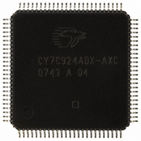
CY7C924ADX-AXC Cypress Semiconductor Corp, CY7C924ADX-AXC Datasheet - Page 7

CY7C924ADX-AXC
Manufacturer Part Number
CY7C924ADX-AXC
Description
IC TXRX HOTLINK 100LQFP
Manufacturer
Cypress Semiconductor Corp
Series
HOTlink™r
Type
Transceiverr
Specifications of CY7C924ADX-AXC
Package / Case
100-LQFP
Protocol
Fibre Channel
Voltage - Supply
4.5 V ~ 5.5 V
Mounting Type
Surface Mount
Product
Framer
Number Of Transceivers
1
Data Rate
622 Mbps
Supply Voltage (max)
5.5 V
Supply Voltage (min)
4.5 V
Supply Current (max)
250 mA
Maximum Operating Temperature
+ 70 C
Minimum Operating Temperature
0 C
Mounting Style
SMD/SMT
Operating Supply Voltage (typ)
5V
Screening Level
Commercial
Pin Count
100
Mounting
Surface Mount
Package Type
TQFP
Operating Supply Voltage (min)
4.5V
Operating Supply Voltage (max)
5.5V
Operating Temperature (min)
0C
Operating Temperature (max)
70C
Ic Interface Type
Parallel, Serial
Supply Voltage Range
4.5V To 5.5V
Operating Temperature Range
0°C To +70°C
Digital Ic Case Style
TQFP
No. Of Pins
100
No. Of Receivers
2
Frequency Max
50MHz
Rohs Compliant
Yes
Termination Type
SMD
Filter Terminals
SMD
Driver Case Style
TQFP
Lead Free Status / RoHS Status
Lead free / RoHS Compliant
Number Of Drivers/receivers
-
Lead Free Status / Rohs Status
Compliant
Other names
428-2918
CY7C924ADX-AXC
CY7C924ADX-AXC
Available stocks
Company
Part Number
Manufacturer
Quantity
Price
Company:
Part Number:
CY7C924ADX-AXC
Manufacturer:
CY
Quantity:
6
Company:
Part Number:
CY7C924ADX-AXC
Manufacturer:
CYPRESS
Quantity:
455
Company:
Part Number:
CY7C924ADX-AXC
Manufacturer:
Cypress Semiconductor Corp
Quantity:
10 000
Document #: 38-02008 Rev. *E
Pin Descriptions
CY7C924ADX HOTLink Transceiver
31
29
23
65
Number
Pin
RXDATA[9]
RXRVS/
RXDATA[10]
RXSOC/
RXDATA[11]
RXSC/D*
Name
(continued)
Bidirectional TTL,
changes following
RXCLK↑, or sampled
by RXCLK↑
Bidirectional TTL,
changes following
RXCLK↑, or sampled
by RXCLK↑, Internal
Pull Up
Bidirectional TTL,
changes following
RXCLK↑, or sampled
by RXCLK↑
Bidirectional TTL,
changes following
RXCLK↑, or sampled
by RXCLK↑
I/O Characteristics
Receive Data Output. When the decoder is enabled in 10 bit mode
(ENCBYP* is HIGH and BYTE8/10* is LOW), this output is the tenth bit (MSB)
of the 10 bit decoded and unpacked data character. When the Decoder is
enabled and in 8 bit mode this output is ignored.
When the Decoder is bypassed (ENCBYP* is LOW), RXDATA[9] functions as
the tenth bit of the 10 or 12 bit undecoded receive character.
Received Violation Symbol Indicator. For data accesses with the Receive
FIFO and decoder are enabled (FIFOBYP* and ENCBYP* are HIGH) this
signal is used as an output. It is decoded in conjunction with RXSC/D* and
RXSOC, according to
Special Character codes in the received data stream. For data accesses with
the Receive FIFO disabled and the Decoder enabled, this output indicates a
code word violation detection on the serial inputs.
When the Decoder is bypassed (ENCBYP* is LOW) and in 10 -bit mode
(BYTE8/10* is LOW), RXDATA[10] functions as the eleventh bit of the 12 bit
undecoded receive character. In 8 bit mode this output is unused and is driven
LOW.
RXRVS reports BIST pattern mismatches when RXBISTEN* is LOW.
When accessing the Serial Address Register, this signal is a “read/write”
control input. RXRVS LOW allows the host system to write the Serial Address
Register (RXDATA[9:0] and RXSC/D* are inputs). RXRVS HIGH allows the
host system to read the Serial Address Register (RXDATA[9:0] and RXSC/D*
are outputs).
Receive Start Of Cell. When the Receive FIFO and decoder are enabled
(FIFOBYP* and ENCBYP* are HIGH), this output is decoded in conjunction
with RXSC/D* and RXRVS, according to
specific Special Character codes in the received data stream.
When the Decoder is bypassed (ENCBYP* is LOW) and in 10 bit mode
(BYTE8/10* is LOW), RXDATA[11] is the twelfth bit (MSB) of the 12 bit
undecoded receive character. In 8 bit mode (BYTE8/10* is HIGH) this output
is unused and is driven LOW.
Received Special Character or Data Indicator. For data accesses with the
Receive FIFO and decoder enabled (FIFOBYP* and ENCBYP* are HIGH) this
signal is an output. It is decoded in conjunction with RXSOC and RXRVS, in
accordance with
Character codes in the received data stream. For data accesses with the
Receive FIFO disabled and the decoder enabled, this output indicates that the
parallel output RXDATA[7:0] is a Special Character code.
When accessing the Serial Address Register, this signal is an input that selects
the addressing mode. RXSC/D* HIGH configures the Serial Address Register
for Unicast address matching. RXSC/D* LOW configures the Serial Address
Register for Multicast address matching.
When operated with the decoder bypassed (ENCBYP* is LOW) this pin has
no function.
Table
Table 6 on page
6, to indicate the presence of specific Special
Signal Description
22, to indicate the presence of specific
Table
6, to indicate the presence of
CY7C924ADX
Page 7 of 58
[+] Feedback


