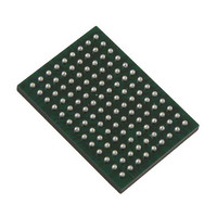
VSC8211XVW Vitesse Semiconductor Corp, VSC8211XVW Datasheet - Page 96

VSC8211XVW
Manufacturer Part Number
VSC8211XVW
Description
IC PHY 10/100/1000 SGL 117-LBGA
Manufacturer
Vitesse Semiconductor Corp
Type
PHY Transceiverr
Specifications of VSC8211XVW
Number Of Drivers/receivers
1/1
Protocol
Gigabit Ethernet
Voltage - Supply
3 V ~ 3.6 V
Mounting Type
Surface Mount
Package / Case
117-LBGA
Case
BGA
Dc
07+
Lead Free Status / RoHS Status
Lead free / RoHS Compliant
Other names
907-1023
Available stocks
Company
Part Number
Manufacturer
Quantity
Price
Company:
Part Number:
VSC8211XVW
Manufacturer:
VITESSE
Quantity:
5
Company:
Part Number:
VSC8211XVW
Manufacturer:
Semtech
Quantity:
3 413
Company:
Part Number:
VSC8211XVW
Manufacturer:
VITESSE
Quantity:
648
Company:
Part Number:
VSC8211XVW
Manufacturer:
Vitesse Semiconductor Corporation
Quantity:
10 000
Part Number:
VSC8211XVW
Manufacturer:
VITESSE
Quantity:
20 000
25.3.10 Register 9 (09h) – 1000BASE-T Control Register
25.3.10.7 Clause 28 View
9.15:13 Transmitter/Receiver Test Mode
This test is valid only in 1000BASE-T mode. Refer to IEEE 802.3-2002, section 40.6.1.1.2 for more information.
• Test Mode 1: The PHY repeatedly transmits the following sequence of data symbols from all four transmitters:
• Test Mode 2: The PHY transmits the data symbol sequence {+2, -2} repeatedly on all channels. The transmitter
1
VMDS-10105 Revision 4.1
October 2006
Bit
15:13 Transmitter Test Mode
12
11
10
9
8
7:0
The state of this register is internally latched when the Auto-Negotiation state machine enters the ABILITY_DETECT state. Changes to the
states of these bits are recognized only at that time. This register is valid only in 1000BASE-T mode.
{{"+2" followed by 127 "0" symbols}, {"-2" followed by 127 "0" symbols}, {"+1" followed by 127 "0" symbols}, {"-1"
followed by 127 "0" symbols}, {128 "+2" symbols, 128 "-2" symbols, 128 "+2" symbols, 128 "-2" symbols}, {1024
"0" symbols}}. The transmitter should use a 125.00 MHz ± 0.01% clock and should operate in MASTER timing
mode.
should use a 125.00 MHz ± 0.01% clock in the MASTER timing mode.
Register 9 (09h) – 1000BASE-T Control Register - Clause 28 View
Name
MASTER/SLAVE Manual
Configuration Enable
MASTER/SLAVE Manual
Configuration Value
Port Type
1000BASE-T FDX Capability
1000BASE-T HDX Capability
Reserved
(9.15)
Bit 1
1
0
0
0
0
1
1
1
1
(9.14)
Bit 2
0
0
1
1
0
0
1
1
1
Access States
R/W
R/W
R/W
R/W
R/W
R/W
R/W
(9.13)
Bit 3
0
1
0
1
0
1
0
1
Normal operation
Test Mode 1 – Transmit waveform test
Test Mode 2 – Transmit jitter test in MASTER mode
Test Mode 3 – Transmit jitter test in SLAVE mode
Test Mode 4 – Transmitter distortion test
Reserved; operation not defined
Reserved; operation not defined
Reserved; operation not defined
Described below, per IEEE 802.3, 40.6.1.1.2
1 = Enable MASTER/SLAVE Manual Configura-
tion value
0 = Disable MASTER/SLAVE Manual Configura-
tion value
1 = Configure PHY as MASTER during MAS-
0 = Configure PHY as SLAVE during MASTER/
1 = Multi-port device
0 = Single-port device
1 = PHY is 1000BASE-T FDX capable
1 = PHY is 1000BASE-T HDX capable
TER/SLAVE negotiation, only when bit 9.12
is set to logical one.
SLAVE negotiation, only when bit 9.12 is set
to logical one.
96 of 165
Test Mode
Reset Value
000
0
0
0
CMODE
CMODE
00000000
Datasheet
VSC8211
Sticky


