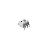
FDS6670S Fairchild Semiconductor, FDS6670S Datasheet - Page 5

FDS6670S
Manufacturer Part Number
FDS6670S
Description
MOSFET Power SO-8
Manufacturer
Fairchild Semiconductor
Specifications of FDS6670S
Configuration
Single Quad Drain Triple Source
Transistor Polarity
N-Channel
Resistance Drain-source Rds (on)
0.009 Ohms
Drain-source Breakdown Voltage
30 V
Gate-source Breakdown Voltage
+/- 20 V
Continuous Drain Current
13.5 A
Power Dissipation
2.5 W
Maximum Operating Temperature
+ 150 C
Mounting Style
SMD/SMT
Package / Case
SOIC-8 Narrow
Minimum Operating Temperature
- 55 C
Lead Free Status / Rohs Status
In Transition
Other names
FDS6670S_NL
Available stocks
Company
Part Number
Manufacturer
Quantity
Price
Part Number:
FDS6670S
Manufacturer:
FAIRCHILD/仙童
Quantity:
20 000
Company:
Part Number:
FDS6670S-NL
Manufacturer:
FAIRCHILD
Quantity:
50 000
Typical Characteristics
0.01
100
10
0.1
10
8
6
4
2
0
1
Figure 9. Maximum Safe Operating Area.
0.01
0
Figure 7. Gate Charge Characteristics.
0.001
0.01
I
0.1
D
R
SINGLE PULSE
R
0.0001
=13.5A
1
DS(ON)
5
JA
V
T
GS
A
= 125
= 25
= 10V
LIMIT
10
o
o
C
C/W
0.1
V
D = 0.5
DS
0.2
, DRAIN-SOURCE VOLTAGE (V)
0.1
0.05
15
0.02
Q
0.01
g
, GATE CHARGE (nC)
0.001
SINGLE PULSE
20
DC
1
Figure 11. Transient Thermal Response Curve.
10s
25
1s
100ms
Thermal characterization performed using the conditions described in Note 1c.
Transient thermal response will change depending on the circuit board design.
(continued)
30
10ms
V
D S
0.01
1ms
= 5V
10
35
100 s
15V
40
10V
100
45
0.1
t
1
, TIME (sec)
3600
3000
2400
1800
1200
600
50
40
30
20
10
0
0.001
0
Figure 8. Capacitance Characteristics.
0
Figure 10. Single Pulse Maximum
1
0.01
5
V
Power Dissipation.
D S
, DRAIN TO SOURCE VOLTAGE (V)
0.1
10
10
C
C
C
t
1
RSS
ISS
OSS
, TIME (sec)
15
1
P(pk)
Duty Cycle, D = t
T
R
R
J
JA
- T
10
100
20
JA
(t) = r(t) + R
A
= 125 °C/W
t
1
SINGLE PULSE
= P * R
R
t
2
JA
T
V
f = 1MHz
A
= 125°C/W
GS
= 25°C
100
FDS6670S Rev E (W)
25
= 0 V
JA
1
JA
(t)
/ t
2
1000
1000
30


