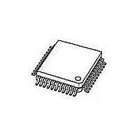
SAK-C505CA-4RM CA Infineon Technologies, SAK-C505CA-4RM CA Datasheet - Page 23

SAK-C505CA-4RM CA
Manufacturer Part Number
SAK-C505CA-4RM CA
Description
Microcontrollers (MCU) 8-Bit Single Chip Microcontroller
Manufacturer
Infineon Technologies
Datasheet
1.SAK-C505CA-4RM_CA.pdf
(88 pages)
Specifications of SAK-C505CA-4RM CA
Data Bus Width
8 bit
Program Memory Type
ROM
Program Memory Size
32 KB
Data Ram Size
1.25 KB
Interface Type
USART
Maximum Clock Frequency
20 MHz
Number Of Programmable I/os
34
Number Of Timers
3
Operating Supply Voltage
5 V
Maximum Operating Temperature
+ 125 C
Mounting Style
SMD/SMT
Package / Case
PG-MQFP-44
Minimum Operating Temperature
- 40 C
On-chip Adc
10 bit, 8 Channel
Packages
PG-MQFP-44
Max Clock Frequency
20.0 MHz
Sram (incl. Cache)
1.25 KByte
Can Nodes
1
A / D Input Lines (incl. Fadc)
8
Program Memory
32.0 KByte
Lead Free Status / Rohs Status
No
Other names
K505CA4RMCANT
Table 3
Special Function Registers - Functional Blocks
Block
CPU
A/D-
Converter
Interrupt
System
XRAM
Data Sheet
1) Bit-addressable special function registers
2) This special function register is listed repeatedly since some bits of it also belong to other functional blocks.
3) “X“ means that the value is undefined and the location is reserved
4) This SFR is a mapped SFR. For accessing this SFR, bit RMAP in SFR SYSCON must be set.
5) The content of this SFR varies with the actual step of the C505 (eg. 01
6) C505 / C505A/C505C only
7) C505CA only
Symbol
ACC
B
DPH
DPL
DPSEL
PSW
SP
SYSCON
VR0
VR1
VR2
ADCON0
ADCON1
ADDAT
ADST
ADDATH
ADDATL
P1ANA
IEN0
IEN1
IP0
IP1
TCON
T2CON
SCON
IRCON
XPAGE
SYSCON
2)
4)
4)
4)
2)
2)
2)
2)
2) 4)
2)
2)
2)
2)
Name
Accumulator
B-Register
Data Pointer, High Byte
Data Pointer, Low Byte
Data Pointer Select Register
Program Status Word Register
Stack Pointer
System Control Register
Version Register 0
Version Register 1
Version Register 2
A/D Converter Control Register 0
A/D Converter Control Register 1
A/D Converter Data Reg. (C505/C505C)
A/D Converter Start Reg. (C505/C505C)
A/D Converter High Byte Data Register
A/D Converter Low Byte Data Register
Port 1 Analog Input Selection Register
Interrupt Enable Register 0
Interrupt Enable Register 1
Interrupt Priority Register 0
Interrupt Priority Register 1
Timer Control Register
Timer 2 Control Register
Serial Channel Control Register
Interrupt Request Control Register
Page Address Register for Extended on-chip
XRAM and CAN Controller
System Control Register
(C505A/C505CA)
(C505A/C505CA)
19
C505/C505C/C505A/C505CA
H
for the first step)
Address Contents after
E0 H
F0 H
83 H
82 H
92 H
D0 H
81 H
B1 H
FC H
FD H
FE H
D8 H
DC H
D9 H
DA H
D9 H
DA H
90 H
A8 H
B8 H
A9 H
B9 H
88 H
C8 H
98 H
C0 H
91 H
B1 H
1)
1)
1)
1)
1)
1)
1)
1)
1)
1)
Reset
00 H
00 H
00 H
00 H
XXXXX000 B
00 H
07 H
XX100X01 B
XX100001 B
C5 H
05 H
5)
00X00000 B
01XXX000 B
00 H
XX H
00 H
00XXXXXX B
FF H
00 H
00 H
00 H
XX000000 B
00 H
00X00000 B
00 H
00 H
00 H
XX100X01 B
XX100001 B
3)
12.00
3) 7)
3)
3)
3) 7)
3) 6)
3)
3) 6)
3)
3)


