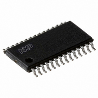
PCA9575PW2,118 NXP Semiconductors, PCA9575PW2,118 Datasheet - Page 10

PCA9575PW2,118
Manufacturer Part Number
PCA9575PW2,118
Description
IC I2C/SMBUS 16BIT GPIO 28-TSSOP
Manufacturer
NXP Semiconductors
Series
-r
Datasheet
1.PCA9575HF118.pdf
(38 pages)
Specifications of PCA9575PW2,118
Interface
I²C, SMBus
Number Of I /o
16
Interrupt Output
Yes
Frequency - Clock
400kHz
Voltage - Supply
1.1 V ~ 3.6 V
Operating Temperature
-40°C ~ 85°C
Mounting Type
Surface Mount
Package / Case
28-TSSOP
Includes
POR
Description/function
16-bit I2C-bus and SMBus
Maximum Operating Temperature
+ 85 C
Minimum Operating Temperature
- 40 C
Mounting Style
SMD/SMT
Supply Voltage (max)
3.6 V
Supply Voltage (min)
1.1 V
Lead Free Status / RoHS Status
Lead free / RoHS Compliant
Other names
935286414118
NXP Semiconductors
Table 3.
PCA9575_3
Product data sheet
Register number
0Dh
0Eh
0Fh
Register summary
7.6.1 Register 0 - Input port 0 register
7.5 Writing to port registers
7.6 Reading the port registers
D3
1
1
1
Data is transmitted to the PCA9575 by sending the device address and setting the least
significant bit to logic 0 (see
is sent after the address and determines which register will receive the data following the
command byte. Each 8-bit register may be updated independently of the other registers.
In order to read data from the PCA9575, the bus master must first send the PCA9575
address with the least significant bit set to a logic 0 (see
address). The command byte is sent after the address and determines which register will
be accessed. After a restart, the device address is sent again but this time, the least
significant bit is set to logic 1. Data from the register defined by the command byte will
then be sent by the PCA9575. Data is clocked into the register on the falling edge of the
acknowledge clock pulse. After the first byte is read, additional bytes may be read using
the auto-increment feature.
This register is read-only. It reflects the incoming logic levels of the pins, regardless of
whether the pin is defined as an input or an output by the Configuration register. Writes to
this register will be acknowledged but will have no effect.
The default ‘X’ is determined by the externally applied logic level.
Table 4.
Bit
7
6
5
4
3
2
1
0
D2
1
1
1
…continued
Symbol
IO0.7
IO0.6
IO0.5
IO0.4
IO0.3
IO0.2
IO0.1
IO0.0
D1
0
1
1
Register 0 - Input port 0 register (address 00h) bit description
D0
1
0
1
Access
read only
read only
read only
read only
read only
read only
read only
read only
Name
MSK1
INTS0
INTS1
Rev. 03 — 9 November 2009
16-bit I
Figure 6
2
Value
X
X
X
X
X
X
X
X
C-bus and SMBus, level translating, low voltage GPIO
Type
read/write
read only
read only
or
Figure 7
Description
determined by externally applied logic level
Function
Interrupt mask port 1 register
Interrupt status port 0 register
Interrupt status port 1 register
for device address). The command byte
Figure 6
or
Figure 7
PCA9575
© NXP B.V. 2009. All rights reserved.
for device
10 of 38


