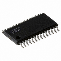
PCA9575PW2,118 NXP Semiconductors, PCA9575PW2,118 Datasheet - Page 7

PCA9575PW2,118
Manufacturer Part Number
PCA9575PW2,118
Description
IC I2C/SMBUS 16BIT GPIO 28-TSSOP
Manufacturer
NXP Semiconductors
Series
-r
Datasheet
1.PCA9575HF118.pdf
(38 pages)
Specifications of PCA9575PW2,118
Interface
I²C, SMBus
Number Of I /o
16
Interrupt Output
Yes
Frequency - Clock
400kHz
Voltage - Supply
1.1 V ~ 3.6 V
Operating Temperature
-40°C ~ 85°C
Mounting Type
Surface Mount
Package / Case
28-TSSOP
Includes
POR
Description/function
16-bit I2C-bus and SMBus
Maximum Operating Temperature
+ 85 C
Minimum Operating Temperature
- 40 C
Mounting Style
SMD/SMT
Supply Voltage (max)
3.6 V
Supply Voltage (min)
1.1 V
Lead Free Status / RoHS Status
Lead free / RoHS Compliant
Other names
935286414118
NXP Semiconductors
PCA9575_3
Product data sheet
6.2 Pin description
Table 2.
[1]
Symbol
A0
V
RESET
P0_0
P0_1
P0_2
P0_3
A1
V
P0_4
P0_5
P0_6
P0_7
INT
A2
V
P1_7
P1_6
P1_5
P1_4
V
A3
P1_3
P1_2
P1_1
P1_0
SDA
SCL
DD
DD(IO)0
SS
DD(IO)1
HWQFN24 package die supply ground is connected to both V
be connected to supply ground for proper device operation. For enhanced thermal, electrical, and board
level performance, the exposed pad needs to be soldered to the board using a corresponding thermal pad
on the board and for proper heat conduction through the board, thermal vias need to be incorporated in the
PCB in the thermal pad region.
Pin
TSSOP28 TSSOP24 HWQFN24
1
2
3
4
5
6
7
8
9
10
11
12
13
14
15
16
17
18
19
20
21
22
23
24
25
26
27
28
Pin description
-
1
2
3
4
5
6
-
7
8
9
10
11
12
-
13
14
15
16
17
18
-
19
20
21
22
23
24
Rev. 03 — 9 November 2009
16-bit I
2
C-bus and SMBus, level translating, low voltage GPIO
-
22
23
24
1
2
3
-
4
5
6
7
8
9
-
10
11
12
13
14
15
-
16
17
18
19
20
21
[1]
Type
I
power supply
I
I/O
I/O
I/O
I/O
I
power supply
I/O
I/O
I/O
I/O
O
I
ground
I/O
I/O
I/O
I/O
power supply
I
I/O
I/O
I/O
I/O
I/O
I
SS
pin and exposed center pad. V
Description
address input 0
supply voltage
active LOW reset input
port 0 input/output 0
port 0 input/output 1
port 0 input/output 2
port 0 input/output 3
address input 1
I/O supply voltage for bank 0
port 0 input/output 0
port 0 input/output 1
port 0 input/output 2
port 0 input/output 3
interrupt output (open-drain;
active LOW)
address input 2
supply ground
port 1 input/output 4
port 1 input/output 5
port 1 input/output 6
port 1 input/output 7
I/O supply voltage for bank 1
address input 3
port 1 input/output 3
port 1 input/output 2
port 1 input/output 1
port 1 input/output 0
serial data line
serial clock line
PCA9575
© NXP B.V. 2009. All rights reserved.
SS
pin must
7 of 38


