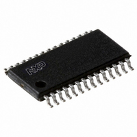
PCA9575PW2,118 NXP Semiconductors, PCA9575PW2,118 Datasheet - Page 19

PCA9575PW2,118
Manufacturer Part Number
PCA9575PW2,118
Description
IC I2C/SMBUS 16BIT GPIO 28-TSSOP
Manufacturer
NXP Semiconductors
Series
-r
Datasheet
1.PCA9575HF118.pdf
(38 pages)
Specifications of PCA9575PW2,118
Interface
I²C, SMBus
Number Of I /o
16
Interrupt Output
Yes
Frequency - Clock
400kHz
Voltage - Supply
1.1 V ~ 3.6 V
Operating Temperature
-40°C ~ 85°C
Mounting Type
Surface Mount
Package / Case
28-TSSOP
Includes
POR
Description/function
16-bit I2C-bus and SMBus
Maximum Operating Temperature
+ 85 C
Minimum Operating Temperature
- 40 C
Mounting Style
SMD/SMT
Supply Voltage (max)
3.6 V
Supply Voltage (min)
1.1 V
Lead Free Status / RoHS Status
Lead free / RoHS Compliant
Other names
935286414118
NXP Semiconductors
PCA9575_3
Product data sheet
7.10 Interrupt output (INT)
7.11 Standby
7.9 Software reset
The Software Reset Call allows all the devices in the I
state value through a specific formatted I
implies that the I
The Software Reset sequence is defined as following:
The open-drain active LOW interrupt is activated when one of the port pins changes state
and the port pin is configured as an input and the interrupt on it is not masked. The
interrupt is deactivated when the port pin input returns to its previous state or the Input
Port register is read. It is highly recommended to program the MSK register, and the CFG
registers during the initialization sequence after power-up, since any change to them
during Normal mode operation may cause undesirable interrupt events to happen.
Remark: Changing an I/O from an output to an input may cause a false interrupt to occur
if the state of the pin does not match the contents of the Input Port register. Only a Read of
the Input Port register that contains the bit(s) image of the input(s) that generated the
interrupt clears the interrupt condition.
The PCA9575 goes into standby when the I
than 2.0 A (typical).
1. A START command is sent by the I
2. The reserved General Call I
3. The PCA9575 device(s) acknowledge(s) after seeing the General Call address
4. Once the General Call address has been sent and acknowledged, the master sends
5. Once the right byte has been sent and correctly acknowledged, the master sends a
is sent by the I
‘0000 0000’ (00h) only. If the R/W bit is set to logic 1 (read), no acknowledge is
returned to the I
1 byte. The value of the byte must be equal to 06h (1000 0011).The PCA9575
acknowledges this value only. If the byte is not equal to 06h, the PCA9575 does not
acknowledge it. If more than 1 byte of data is sent, the PCA9575 does not
acknowledge anymore.
STOP command to end the Software Reset sequence: the PCA9575 then resets to
the default value (power-up value) and is ready to be addressed again within the
specified bus free time. If the master sends a Repeated START instead, no reset is
performed. The I
(at any time) as a ‘Software Reset Abort’. The PCA9575 does not initiate a software
reset.
2
C-bus is functional and that there is no device hanging the bus.
2
C-bus master.
2
2
C-bus master.
Rev. 03 — 9 November 2009
C-bus master must interpret a non-acknowledge from the PCA9575
16-bit I
2
2
C-bus and SMBus, level translating, low voltage GPIO
C-bus address ‘0000 000’ with the R/W bit set to 0 (write)
2
C-bus master.
2
C-bus command. To be performed correctly, it
2
C-bus is idle. Standby supply current is lower
2
C-bus to be reset to the power-up
PCA9575
© NXP B.V. 2009. All rights reserved.
19 of 38


