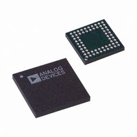
AD9929BBCZ Analog Devices Inc, AD9929BBCZ Datasheet - Page 12

AD9929BBCZ
Manufacturer Part Number
AD9929BBCZ
Description
IC CCD SIGNAL PROCESSOR 64-BGA
Manufacturer
Analog Devices Inc
Type
CCD Signal Processor, 12-Bitr
Datasheet
1.AD9929BBCZ.pdf
(64 pages)
Specifications of AD9929BBCZ
Input Type
Logic
Output Type
Logic
Interface
3-Wire Serial
Mounting Type
Surface Mount
Package / Case
64-CSPBGA
Analog Front End Type
CCD
Analog Front End Category
Video
Interface Type
Serial (3-Wire)
Input Voltage Range
0.5V
Operating Supply Voltage (min)
2.7V
Operating Supply Voltage (typ)
3V
Operating Supply Voltage (max)
3.6V
Resolution
12b
Number Of Adc's
1
Power Supply Type
Analog/Digital
Operating Temp Range
-20C to 85C
Operating Temperature Classification
Commercial
Mounting
Surface Mount
Pin Count
64
Package Type
CSPBGA
Number Of Channels
1
Lead Free Status / RoHS Status
Lead free / RoHS Compliant
Current - Supply
-
Lead Free Status / RoHS Status
Compliant, Lead free / RoHS Compliant
Available stocks
Company
Part Number
Manufacturer
Quantity
Price
Company:
Part Number:
AD9929BBCZ
Manufacturer:
ADI
Quantity:
531
AD9929
Address
0x0A
(VD
SyncReg)
0x0B
(VD
SyncReg)
0x0C
(VD
SyncReg)
0x0D
(VD
SyncReg)
0x0E
(VD
SyncReg)
0x0F
0x17
0x18
0x19
0x1A
1
1
1
1
1
Content
23
22
(21:16)
(15:12)
(11:10)
9
8
(7:4)
(3:2)
1
0
(23:22)
21
20
(19:17)
16
15
(14:12)
11
(10:0)
(23:21)
20
(19:18)
17
16
15
(14:12)
11
(10:0)
(23:17)
16
(15:11)
(10:0)
(23:22)
(21:20)
(19:18)
17
16
(15:10)
(9:0)
(23:8)
(7:0)
(23:13)
(12:0)
(23:13)
(12:0)
(23:13)
(12:0)
(23:13)
(12:0)
Bit
Width
1
1
6
4
2
1
1
4
2
1
1
2
1
1
3
1
1
3
1
11
3
1
2
1
1
1
3
1
11
7
1
5
11
2
2
2
1
1
6
10
16
8
11
13
11
13
11
13
11
13
Default
Value
0
0
0x00
0
0
0
0
C
3
0
0
0
1
1
0
0
0
0
0
0x7FF
0
0
0
0
0
0
0
0
0x000
–
0
–
0x000
0
0
0
0
0
0x00
0x000
0
60
–
0x1FFF
–
0x1FFF
–
0x1FFF
–
0x1FFF
Register Name
Unused
FDPOL
XVSGMASK
SYNCCNT
SVREP_MODE
HBLKEXT
HPULSECNT
SPATLOGIC
SVOS
SPAT_EN
MODE
Unused
XSUBCK_EN
XVSG_EN
Unused
STROBE_EN
Unused
XSUBCKNUM_HP
Unused
XSUBCKNUM
Unused
MSHUTINIT
Unused
Unused
MSHUTEN
Unused
MSHUTPOS_HP
Unused
MSHUTPOS
Unused
VSUBPOL
Unused
VSUBTOG
Unused
TESTMODE1
Unused
TESTMODE2
TESTMODE3
Unused
VGAGAIN
Unused
XVSGLEN_1
Unused
XV1SPAT_TOG1
Unused
XV1SPAT_TOG2
Unused
XV2SPAT_TOG1
Unused
XV2SPAT_TOG2
Rev. A | Page 12 of 64
Register Description
FD Polarity Control (0 = Low, 1 = High)
XVSG Masking (See Table 25)
External SYNC Setting
Super Vertical Repetition Mode
H Pulse Blanking Extend Control
H Pulse Control During Blanking
SPAT Logic Setting (See Table 27)
Second V Output Setting (10 = Ouput Repetition 1)
SPAT Control (0 = SPAT Disable, 1 = SPAT Enable)
Mode Control Bit (0 = Mode_A, 1 = Mode_B)
XSUBCK Output Enable Control (0 = Disable, 1 = Enable)
XVSG Output Enable Control (0 = Disable, 1 = Enable)
STROBE Output Control (0 = STROBE Output Held Low,
1 = STROBE Output Enabled)
High Precision Shutter XSUBCLK Pulse Position/Number
Total Number of XSUBCKs Per Field
MSHUT Initialize (1 = Forces MSHUT Low)
MSHUT Control (0 = MSHUT Held at Last State, 1 = MSHUT Output)
MSHUT Position during High Precision Operation
MSHUT Position during Normal Operation
VSUB Active Polarity (0 = Low, 1 = High)
VSUB Toggle Position. Active Starting Line in any Field.
This Register Should Always Be Set = 0.
This Register Should Always Be Set = 0.
This Register Should Always Be Set = 0.
VGA Gain
XVSGTOG_1 Pulse Width
XV1SPAT Toggle Position #1 (Mode_A Active)
XV1SPAT Toggle Position #2 (Mode_A Active)
XV2SPAT Toggle Position #1 (Mode_A Active)
XV2SPAT Toggle Position #2 (Mode_A active)


