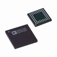
AD9929BBCZ Analog Devices Inc, AD9929BBCZ Datasheet - Page 60

AD9929BBCZ
Manufacturer Part Number
AD9929BBCZ
Description
IC CCD SIGNAL PROCESSOR 64-BGA
Manufacturer
Analog Devices Inc
Type
CCD Signal Processor, 12-Bitr
Datasheet
1.AD9929BBCZ.pdf
(64 pages)
Specifications of AD9929BBCZ
Input Type
Logic
Output Type
Logic
Interface
3-Wire Serial
Mounting Type
Surface Mount
Package / Case
64-CSPBGA
Analog Front End Type
CCD
Analog Front End Category
Video
Interface Type
Serial (3-Wire)
Input Voltage Range
0.5V
Operating Supply Voltage (min)
2.7V
Operating Supply Voltage (typ)
3V
Operating Supply Voltage (max)
3.6V
Resolution
12b
Number Of Adc's
1
Power Supply Type
Analog/Digital
Operating Temp Range
-20C to 85C
Operating Temperature Classification
Commercial
Mounting
Surface Mount
Pin Count
64
Package Type
CSPBGA
Number Of Channels
1
Lead Free Status / RoHS Status
Lead free / RoHS Compliant
Current - Supply
-
Lead Free Status / RoHS Status
Compliant, Lead free / RoHS Compliant
Available stocks
Company
Part Number
Manufacturer
Quantity
Price
Company:
Part Number:
AD9929BBCZ
Manufacturer:
ADI
Quantity:
531
AD9929
CIRCUIT LAYOUT INFORMATION
The AD9929 typical circuit connection is shown in Figure 71.
The PCB layout is critical in achieving good image quality from
the AD9929 product. All of the supply pins must be decoupled
to ground with good quality, high frequency chip capacitors.
The 0.1 µF decoupling capacitors should be located as close as
possible to the supply pins, and should have a very low induc-
tance path to a continuous ground plane. There should also be a
4.7 µF or larger capacitor for each main supply, although it is
not necessary for each individual pin.
In most applications it is easier and recommended to share the
same supply for AVDD, DVDD, TCVDD, RGVDD, and HVDD,
as long as the individual supply pins are separately bypassed at
each supply pin. A separate 3 V supply should be used for
DRVDD with this supply pin decoupled to the same ground
plane as the rest of the chip. A separate ground for DRVSS is not
recommended.
The vertical driver VM supply pins can be connected to indi-
vidual supplies or to the same supply, depending on the appli-
cation requirement for the mid-level voltage on the vertical
outputs. These pins may also be directly connected to the
common ground plane, as shown in Figure 71.
Rev. A | Page 60 of 64
The analog bypass pins, REFB, REFT, should also be carefully
decoupled to ground as close as possible to their respective pins.
The analog input, CCDIN, capacitor should also be located
close to the pin.
The H1, H2, and RG printed circuit board traces should be
designed to have low inductance to avoid excessive distortion of
the signals. Heavier traces are recommended because of the
large transient current demand by the CCD on H1 and H2. If
possible, physically locate the AD9929 close to the CCD to
reduce the inductance on these lines. As always, the routing
path should be as direct as possible from the AD9929 to the
CCD. Careful trace impedance considerations must also be
made with applications using a flex printed circuit (FPC) con-
necting the CCD to the AD9929. FPC trace impedances can be
controlled by applying a solid uniform ground plane under the
H1, H2, and RG traces. This helps minimize the amount of
overshoot and ringing on these signals at the CCD inputs.


