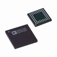
AD9929BBCZ Analog Devices Inc, AD9929BBCZ Datasheet - Page 13

AD9929BBCZ
Manufacturer Part Number
AD9929BBCZ
Description
IC CCD SIGNAL PROCESSOR 64-BGA
Manufacturer
Analog Devices Inc
Type
CCD Signal Processor, 12-Bitr
Datasheet
1.AD9929BBCZ.pdf
(64 pages)
Specifications of AD9929BBCZ
Input Type
Logic
Output Type
Logic
Interface
3-Wire Serial
Mounting Type
Surface Mount
Package / Case
64-CSPBGA
Analog Front End Type
CCD
Analog Front End Category
Video
Interface Type
Serial (3-Wire)
Input Voltage Range
0.5V
Operating Supply Voltage (min)
2.7V
Operating Supply Voltage (typ)
3V
Operating Supply Voltage (max)
3.6V
Resolution
12b
Number Of Adc's
1
Power Supply Type
Analog/Digital
Operating Temp Range
-20C to 85C
Operating Temperature Classification
Commercial
Mounting
Surface Mount
Pin Count
64
Package Type
CSPBGA
Number Of Channels
1
Lead Free Status / RoHS Status
Lead free / RoHS Compliant
Current - Supply
-
Lead Free Status / RoHS Status
Compliant, Lead free / RoHS Compliant
Available stocks
Company
Part Number
Manufacturer
Quantity
Price
Company:
Part Number:
AD9929BBCZ
Manufacturer:
ADI
Quantity:
531
Address
0x1B
0x1C
0x1D
0x1E
0x1F
0x20
0x21
0x22
0x23
0x24
0x25
0x26
0xD5
0xD6
1
This register defaults to VD synchronous mode type at power-up. VD sync type registers do not get updated until the first falling edge of VD is asserted after the
register has been programmed. VD sync type registers can be programmed to be asynchronous registers by setting VDMODE = 1 (Address 0x01).
Content
(23:13)
(12:0)
(23:13))
(12:0
(23:13)
(12:0)
(23:13)
(12:0)
(23:13)
(12:0)
(23:13)
(12:0)
(23:13)
(12:0)
(23:13)
(12:0)
(23:13)
(12:0)
(23:13)
(12:0)
(23:13)
(12:0)
(23:13)
(12:0)
(23:4)
3
2
(1:0)
(23:1)
0
Bit
Width
11
13
11
13
11
13
11
13
11
13
11
13
11
13
11
13
11
13
11
13
11
13
11
13
20
1
1
2
23
1
Default
Value
–
0x1FFF
–
0x1FFF
–
0x1FFF
–
0x1FFF
–
0x1FFF
–
0x1FFF
–
0x1FFF
–
0x1FFF
–
0x1FFF
–
0x1FFF
–
0x1FFF
–
0x1FFF
0x00000
1
0
0
0x000000
1
Register Name
Unused
XV3SPAT_TOG1
Unused
XV3SPAT_TOG2
Unused
XV4SPAT_TOG1
Unused
XV4SPAT_TOG2
Unused
XV1SPAT_TOG1
Unused
XV1SPAT_TOG2
Unused
XV2SPAT_TOG1
Unused
XV2SPAT_TOG2
Unused
XV3SPAT_TOG1
Unused
XV3SPAT_TOG2
Unused
XV4SPAT_TOG1
Unused
XV4SPAT_TOG2
Unused
DCLK2SEL
DCLK1SEL
CLKDIV
Unused
SLAVE_MODE
Rev. A | Page 13 of 64
Register Description
XV3SPAT Toggle Position #1 (Mode_A active)
XV3SPAT Toggle Position #2 (Mode_A active)
XV4SPAT Toggle Position #1 (Mode_A active)
XV4SPAT Toggle Position #2 (Mode_A Active)
XV1SPAT Toggle Position #1 (Mode_A Active)
XV1SPAT Toggle Position #2 (Mode_B Active)
XV2SPAT Toggle Position #1 (Mode_B Active)
XV2SPAT Toggle Position #2 (Mode_B Active)
XV3SPAT Toggle Position #1 (Mode_B Active)
XV3SPAT Toggle Position #2 (Mode_B Active)
XV4SPAT Toggle Position #1 (Mode_B Active)
XV4SPAT Toggle Position #2 (Mode_B Active)
DCLK2 Selector (0 = Select Internal FD Signal To Be Output on
FD/DCLK2 Pin 16, 1 = Select CLI To Be Output on FD/DCLK2 Pin 16)
DCLK1 Selector (0 = Select DLL Version for DCLK1 Output, 1 = Select
CLI for DCLK1 Output)
Input Clock Divider (0 = No Division, 1 = 1/2, 2 = 1/3, 3 = 1/4)
Operating Mode ( 0 = Master Mode, 1 = Slave Mode)
AD9929


