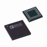
AD9929BBCZ Analog Devices Inc, AD9929BBCZ Datasheet - Page 39

AD9929BBCZ
Manufacturer Part Number
AD9929BBCZ
Description
IC CCD SIGNAL PROCESSOR 64-BGA
Manufacturer
Analog Devices Inc
Type
CCD Signal Processor, 12-Bitr
Datasheet
1.AD9929BBCZ.pdf
(64 pages)
Specifications of AD9929BBCZ
Input Type
Logic
Output Type
Logic
Interface
3-Wire Serial
Mounting Type
Surface Mount
Package / Case
64-CSPBGA
Analog Front End Type
CCD
Analog Front End Category
Video
Interface Type
Serial (3-Wire)
Input Voltage Range
0.5V
Operating Supply Voltage (min)
2.7V
Operating Supply Voltage (typ)
3V
Operating Supply Voltage (max)
3.6V
Resolution
12b
Number Of Adc's
1
Power Supply Type
Analog/Digital
Operating Temp Range
-20C to 85C
Operating Temperature Classification
Commercial
Mounting
Surface Mount
Pin Count
64
Package Type
CSPBGA
Number Of Channels
1
Lead Free Status / RoHS Status
Lead free / RoHS Compliant
Current - Supply
-
Lead Free Status / RoHS Status
Compliant, Lead free / RoHS Compliant
Available stocks
Company
Part Number
Manufacturer
Quantity
Price
Company:
Part Number:
AD9929BBCZ
Manufacturer:
ADI
Quantity:
531
SPECIAL VERTICAL SWEEP MODE OPERATION
The AD9929 contains a special mode of vertical timing oper-
ation called sweep mode. This mode is used to generate a
continuous number of repetitive vertical pulses that span
multiple HD lines. One example of where this mode may be
needed is at the start of the CCD readout operation. At the end
of the image exposure, but before the image is transferred by the
sensor gate pulses, the vertical interline CCD registers should be
clean of all charge. This can be accomplished by quickly shifting
out any charge with a long series of pulses on the V1 to V4
outputs. This operation spans multiple HD line lengths.
Normally the sequences are contained within one HD line
length but with the sweep mode enabled, the HD boundaries
will be ignored until the region is finished.
The special vertical sweep mode operation is only output in
CCD Region 0 and CCD Region 3 (see Figure 34), as shown in
Figure 37 and Figure 38. The SVREP_MODE register located at
XV1–XV4
XV1–XV4
XV1–XV4
XV1–XV4
Figure 35. Nonoverlapping Example while Operating in Normal Vertical Timing Operation SVREP_MODE = 0 and VTPREPx = 4
HD
Figure 36. Overlapping Example while Operating in Normal Vertical Timing Operation SVREP_MODE = 0 and VTPREPx = 8
HD
HD
HD
SCP3
SCP0
0
0
Figure 37. Sweep Mode Timing Example with SVREP_MODE = 1 and SVREP0 = 28
Figure 38. Sweep Mode Timing Example with SVREP_MODE = 2 and SVREP3 = 28
1
1
Rev. A | Page 39 of 64
CCD REGION 3
CCD REGION 0
NOT OUTPUT BECAUSE THE 8TH
REPETITION OVERLAPS WITH HD
Control Address 0x0A is used to enable and configure the
special sweep mode operation, as described in Table 25.
The maximum number of repeats in each region is 2048 while
operating in this mode using the SVREP0 and SVREP3
Mode_Reg(4) registers.
Table 25. Description of SVREP_MODE Register
SVREP_MODE
0
0
1
1
2
2
Description of Sweep Mode Operation
0
1
0
1
Normal Vertical Timing Operation in
all CCD Regions
Special Vertical Sweep Mode Timing
Output in CCD Region 0 Only
Special Vertical Sweep Mode Timing
Output in CCD Region 3 Only
Special Vertical Sweep Mode Timing
Output in CCD Region0 and CCD
Region 3
SCP4 = 3
SCP1 = 3
0
0
AD9929


