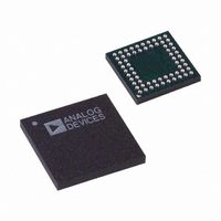
AD9929BBCZ Analog Devices Inc, AD9929BBCZ Datasheet - Page 19

AD9929BBCZ
Manufacturer Part Number
AD9929BBCZ
Description
IC CCD SIGNAL PROCESSOR 64-BGA
Manufacturer
Analog Devices Inc
Type
CCD Signal Processor, 12-Bitr
Datasheet
1.AD9929BBCZ.pdf
(64 pages)
Specifications of AD9929BBCZ
Input Type
Logic
Output Type
Logic
Interface
3-Wire Serial
Mounting Type
Surface Mount
Package / Case
64-CSPBGA
Analog Front End Type
CCD
Analog Front End Category
Video
Interface Type
Serial (3-Wire)
Input Voltage Range
0.5V
Operating Supply Voltage (min)
2.7V
Operating Supply Voltage (typ)
3V
Operating Supply Voltage (max)
3.6V
Resolution
12b
Number Of Adc's
1
Power Supply Type
Analog/Digital
Operating Temp Range
-20C to 85C
Operating Temperature Classification
Commercial
Mounting
Surface Mount
Pin Count
64
Package Type
CSPBGA
Number Of Channels
1
Lead Free Status / RoHS Status
Lead free / RoHS Compliant
Current - Supply
-
Lead Free Status / RoHS Status
Compliant, Lead free / RoHS Compliant
Available stocks
Company
Part Number
Manufacturer
Quantity
Price
Company:
Part Number:
AD9929BBCZ
Manufacturer:
ADI
Quantity:
531
THEORY OF OPERATION
MODES OF OPERATION
Slave and Master Mode Operation
The AD9929 can be operated in either slave or master mode.
It defaults to slave mode operation at power-up. The
SLAVE_MODE register (Address 0xD6) can be used to
configure the AD9929 into master mode by setting
SLAVE_MODE = 0.
Slave Mode Operation
While operating in slave mode, VD, HD, and VGATE are pro-
vided externally from the image processor. VGATE is input
active high on Pin 45.
Unlike master mode operation, there is a 7 CLI clock cycle delay
from the falling edge of HD to when the 12-bit gray code H
counter is reset to 0 (See Figure 62).
Master Mode Operation
While operating in master mode, VD and HD are outputs
and the SYNC/VGATE pin is configured for an external
SYNC input. Master mode is selected by setting register
SLAVE_MODE (Address 0x06) = 0.
HORIZONTAL AND VERTICAL COUNTERS
Figure 8 and Figure 9 show the horizontal and vertical counter
dimensions for the AD9929. All internal horizontal and vertical
clocking is programmed using these dimensions to specify line
and pixel locations.
CLI INPUT CLOCK DIVIDER
The AD9929 provides the capability of dividing the CLI input
clock using Register CLKDIV (Address 0xD5). The following
procedure must be followed to reset the AFE and digital circuits
when CLKDIV is reprogrammed back to 0 from CLKDIV = 1,
2, or 3. The DCLK1 output becomes unstable if this procedure
isn’t followed.
Step 1: CLKDIV = 1, 2, or 3 (CLI divided by setting value)
Step 2: CLKDIV = 0 (CLI reprogrammed for no division)
Step 3: DIGSTBY = AFESTBY = 0
Step 4: DIGSTBY = AFESTBY = 1
CLI
HD
VD
MAX VD LENGTH IS 2048 LINES
MAX HD LENGTH IS 4095 PIXELS
Figure 9. Maximum VD/HD Dimensions
Rev. A | Page 19 of 64
GRAY CODE REGISTERS
See Table 12 for a list of the AD9929 registers requiring gray
code values. The following is an example of applying a gray
code number for HDLEN using a line length of 1560 pixels:
HDLEN = (1560–4) = 1556
HDLEN Register section).
Where 1556
The gray code value of Address 0x51E would be programmed in
the 12-bit HDLEN register.
Table 12. AD9929 Gray Code Registers
Register Name
HDLEN
CLPOBTOG1
CLPOBTOG2
HDLASTLEN
12-BIT HORIZONTAL COUNTER = 4096 PIXELS MAX
10
= Address 0x51E
Figure 8. Horizontal and Vertical Counters
MAXIMUM FIELD DIMENSIONS
10
(see Special Note about the
Register Type
System_Reg(12)
System_Reg(15)
System_Reg(16)
Mode_Reg(1)
AD9929


