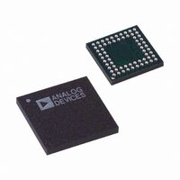
AD9929BBCZ Analog Devices Inc, AD9929BBCZ Datasheet - Page 49

AD9929BBCZ
Manufacturer Part Number
AD9929BBCZ
Description
IC CCD SIGNAL PROCESSOR 64-BGA
Manufacturer
Analog Devices Inc
Type
CCD Signal Processor, 12-Bitr
Datasheet
1.AD9929BBCZ.pdf
(64 pages)
Specifications of AD9929BBCZ
Input Type
Logic
Output Type
Logic
Interface
3-Wire Serial
Mounting Type
Surface Mount
Package / Case
64-CSPBGA
Analog Front End Type
CCD
Analog Front End Category
Video
Interface Type
Serial (3-Wire)
Input Voltage Range
0.5V
Operating Supply Voltage (min)
2.7V
Operating Supply Voltage (typ)
3V
Operating Supply Voltage (max)
3.6V
Resolution
12b
Number Of Adc's
1
Power Supply Type
Analog/Digital
Operating Temp Range
-20C to 85C
Operating Temperature Classification
Commercial
Mounting
Surface Mount
Pin Count
64
Package Type
CSPBGA
Number Of Channels
1
Lead Free Status / RoHS Status
Lead free / RoHS Compliant
Current - Supply
-
Lead Free Status / RoHS Status
Compliant, Lead free / RoHS Compliant
Available stocks
Company
Part Number
Manufacturer
Quantity
Price
Company:
Part Number:
AD9929BBCZ
Manufacturer:
ADI
Quantity:
531
WRITES
VSUB TIMING
The CCD readout bias (VSUB) can be programmed to accom-
modate different CCDs. VSUB on and off toggle positions and
polarity are controlled using VSUBTOG (Address 0x0D) and
VSUBPOL (Address 0x0D) registers, respectively, as described
in Table 36. Since the VSUBTOG is an 11-bit register, the VSUB
on position is programmable within any line. Figure 56 shows
an example of controlling VSUB using these registers.
Table 36. VSUB Registers
Register
Name
VSUBPOL
VSUBTOG
SERIAL
VSUB
VD
HD
1
Bit
Width
1
11
ST COUNTER
XVSGTOG_0
XVSGTOG_1
2
(FIXED)
13-BIT
2 LINES
VD
HD
Register
Type
Control
Control
NOTES
1. XVSGTOG_x (x = 0, 1) REFERENCES THE 13-BIT ST COUNTER
2. XVSGACTLINE (PROGRAMMABLE AT MODE_REG(1))
3. XVSGLEN (PROGRAMMABLE AT SYS_REG(14))
PROGRAMMABLE CLOCK POSITIONS
1. XVSGTOG_0 (PROGRAMMABLE AT SYS_REG(13))
2. XVSGTOG_1 (PROGRAMMABLE AT SYS_REG(13))
0
3
Range
(Lines)
–
0–2048
1
Description
(0 = Low,
1 = High)
VSUB toggle
position
XVSGACTLINE
Figure 56. VSUB Timing Example
Figure 55. Example of VSG Pulse
Rev. A | Page 49 of 64
2
VSUB Placement and Polarity
Figure 56 shows the sequence of events for programming the
VSUB on and off toggle positions and polarity.
1.
2.
3.
4.
5.
6.
Program VSUBTOG = 2 and VSUBPOL = 1.
Since the VSUBTOG and VSUBPOL are VD synchronous
type registers, the falling edge of VD updates the serial
writes from Step 1.
VSUB is asserted high after two HD cycles.
Program VSUBTOG = 3 and VSUBPOL = 0.
Since the VSUBTOG and VSUBPOL are VD synchronous
type registers, the falling edge of VD updates the serial
writes from Step 4.
VSUB is asserted low after three HD cycles.
3
4
XVSGLEN_0
XVSGLEN_1
1
2
5
3 LINES
6
AD9929


