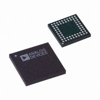
AD9929BBCZ Analog Devices Inc, AD9929BBCZ Datasheet - Page 38

AD9929BBCZ
Manufacturer Part Number
AD9929BBCZ
Description
IC CCD SIGNAL PROCESSOR 64-BGA
Manufacturer
Analog Devices Inc
Type
CCD Signal Processor, 12-Bitr
Datasheet
1.AD9929BBCZ.pdf
(64 pages)
Specifications of AD9929BBCZ
Input Type
Logic
Output Type
Logic
Interface
3-Wire Serial
Mounting Type
Surface Mount
Package / Case
64-CSPBGA
Analog Front End Type
CCD
Analog Front End Category
Video
Interface Type
Serial (3-Wire)
Input Voltage Range
0.5V
Operating Supply Voltage (min)
2.7V
Operating Supply Voltage (typ)
3V
Operating Supply Voltage (max)
3.6V
Resolution
12b
Number Of Adc's
1
Power Supply Type
Analog/Digital
Operating Temp Range
-20C to 85C
Operating Temperature Classification
Commercial
Mounting
Surface Mount
Pin Count
64
Package Type
CSPBGA
Number Of Channels
1
Lead Free Status / RoHS Status
Lead free / RoHS Compliant
Current - Supply
-
Lead Free Status / RoHS Status
Compliant, Lead free / RoHS Compliant
Available stocks
Company
Part Number
Manufacturer
Quantity
Price
Company:
Part Number:
AD9929BBCZ
Manufacturer:
ADI
Quantity:
531
AD9929
Register Name
VTPLEN3
Table 23. Mode_A and Mode_B Registers for VTPx Selection
Register
Name
VTPSEQPTR0
VTPSEQPTR1
VTPSEQPTR2
VTPSEQPTR3
VTPSEQPTR4
VTPSEL0
VTPSEL1
VTPSEL2
VTPSEL3
VTPREP0
VTPREP1
VTPREP2
VTPREP3
1
Table 24. Mode_A and Mode_B Registers for CCD Region Selection
Register Name
SCP1
SCP2
SCP3
SCP4
Register settings 6 and 7 are not used.
XV1STARTPOL3
XV2STARTPOL3
XV3STARTPOL3
XV4STARTPOL3
XV1TOG1POS3
XV1TOG2POS3
XV2TOG1POS3
XV2TOG2POS3
XV3TOG1POS3
XV3TOG2POS3
XV4TOG1POS3
XV4TOG2POS3
1
1
1
1
1
Bit
Width
3
3
3
3
3
2
2
2
2
3
3
3
3
Bit
Width
9
1
1
1
1
9
9
9
9
9
9
9
9
Bit Width
8
8
8
8
Register
Type
Mode_Reg(2)
Mode_Reg(2)
Mode_Reg(2)
Mode_Reg(2)
Mode_Reg(2)
Mode_Reg(3)
Mode_Reg(3)
Mode_Reg(3)
Mode_Reg(3)
Mode_Reg(3)
Mode_Reg(4)
Mode_Reg(4)
Mode_Reg(4)
Register Type
Sys_Reg(9)
Sys_Reg(9)
Sys_Reg(9)
Sys_Reg(9)
Sys_Reg(9)
Sys_Reg(9)
Sys_Reg(9)
Sys_Reg(9 &10)
Sys_Reg(10)
Sys_Reg(10)
Sys_Reg(10&11)
Sys_Reg(11)
Sys_Reg(11)
Register Type
Mode_Reg(2)
Mode_Reg(2)
Mode_Reg(2)
Mode_Reg(2)
Range
0–7
0–7
0–7
0–7
Reference
Counter
V Counter
V Counter
V Counter
V Counter
V Counter
V Counter
V Counter
V Counter
V Counter
Description
Vertical Transfer Pulse Pointer used in CCD Region 0 (0 = VTPSEL0, 1 = VTPSEL1,
2 = VTPSEL2, 3 = VTPSEL3, 4 = VTPSEL0 for Even Line and VTPSEL1 for
Odd Line, 5 = VTPSEL2 for Even Line and VTPSEL3 for Odd Line)
Vertical Transfer Pulse Pointer used in CCD Region 1 (0 = VTPSEL0, 1 = VTPSEL1,
2 = VTPSEL2, 3 = VTPSEL3, 4 = VTPSEL0 for Even Line and VTPSEL1 for
Odd Line, 5 = VTPSEL2 for Even Line and VTPSEL3 for Odd Line)
Vertical Transfer Pulse Pointer used in CCD Region 2 (0 = VTPSEL0, 1 = VTPSEL1,
2 = VTPSEL2, 3 = VTPSEL3, 4 = VTPSEL0 for Even Line and VTPSEL1 for
Odd Line, 5 = VTPSEL2 for Even Line and VTPSEL3 for Odd Line)
Vertical Transfer Pulse Pointer used in CCD Region 3 (0 = VTPSEL0, 1 = VTPSEL1,
2 = VTPSEL2, 3 = VTPSEL3, 4 = VTPSEL0 for Even Line and VTPSEL1 for
Odd Line, 5 = VTPSEL2 for Even Line and VTPSEL3 for Odd Line)
Vertical Transfer Pulse Pointer used in CCD Region 4 (0 = VTPSEL0, 1 = VTPSEL1,
2 = VTPSEL2, 3 = VTPSEL3, 4 = VTPSEL0 for Even Line and VTPSEL1 for
Odd Line, 5 = VTPSEL2 for Even Line and VTPSEL3 for Odd Line)
0 = VTP0, 1 = VTP1, 2 = VTP2, 3 = VTP3
0 = VTP0, 1 = VTP1, 2 = VTP2, 3 = VTP3
0 = VTP0, 1 = VTP1, 2 = VTP2, 3 = VTP3
0 = VTP0, 1 = VTP1, 2 = VTP2, 3 = VTP3
Number of VTP0 Pulse Repetitions within a Line
Number of VTP1 Pulse Repetitions within a Line
Number of VTP2 Pulse Repetitions within a Line
Number of VTP3 Pulse Repetitions within a Line
Rev. A | Page 38 of 64
Range
0–512
High/Low
High/Low
High/Low
High/Low
0–511
0–511
0–511
0–511
0–511
0–511
0–511
0–511
Range
0–255 lines
0–255 lines
0–255 lines
0–255 lines
Description
Length between Repetitions
XV1 Starting Polarity for VTP3
(0 = Low, 1 = High)
XV1 Starting Polarity for VTP3
(0 = Low, 1 = High)
XV1 Starting Polarity for VTP3
(0 = Low, 1 = High)
XV1 Starting Polarity for VTP3
(0 = Low, 1 = High)
XV1 Toggle Position 1 for VTP3
XV1 Toggle Position 2 for VTP3
XV2 Toggle Position 1 for VTP3
XV2 Toggle Position 2 for VTP3
XV3 Toggle Position 1 for VTP3
XV3 Toggle Position 2 for VTP3
XV3 Toggle Position 1 for VTP3
XV3 Toggle Position 2 for VTP3
Description
Sequence Change Position 1
Sequence Change Position 2
Sequence Change Position 3
Sequence Change Position 4
VTP
Pattern
VTP3


