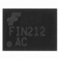
FIN212ACGFX Fairchild Semiconductor, FIN212ACGFX Datasheet - Page 3

FIN212ACGFX
Manufacturer Part Number
FIN212ACGFX
Description
IC SER/DESER 12BIT 42USS-BGA
Manufacturer
Fairchild Semiconductor
Series
SerDes™r
Datasheet
1.FIN212ACGFX.pdf
(16 pages)
Specifications of FIN212ACGFX
Function
Serializer/Deserializer
Data Rate
560Mbps
Input Type
LVCMOS
Output Type
LVCMOS
Number Of Inputs
12
Number Of Outputs
12
Voltage - Supply
1.65 V ~ 3.6 V
Operating Temperature
-30°C ~ 70°C
Mounting Type
Surface Mount
Package / Case
42-BGA
Lead Free Status / RoHS Status
Lead free / RoHS Compliant
Other names
FIN212ACGFXTR
Available stocks
Company
Part Number
Manufacturer
Quantity
Price
Company:
Part Number:
FIN212ACGFX
Manufacturer:
FSC
Quantity:
4 964
Company:
Part Number:
FIN212ACGFX
Manufacturer:
Fairchild Semiconductor
Quantity:
10 000
FIN212AC (Deserializer DIRI=0) Pin Descriptions
Note:
2.
FIN212AC (Deserializer DIRI=0) Pin Configurations
© 2008 Fairchild Semiconductor Corporation
FIN212AC • Rev. 1.1.0
Pin Name
DIRI
XTERM
S0
S1
PWS0
PWS1
DP[1:12]
CKP
DSI+
DSI-
CKSI+
CKSI-
CKSO+
CKSO-
CKREF
STROBE
/DIRO
VDDP
VDDS
VDDA
GND
N/C
C
D
G
A
B
E
F
0=GND; 1=VDDP
42-Ball BGA, 3.5 x 4.5mm, .5mm pitch (Top View)
DP[10]
DP[12]
DP[4]
DP[6]
DP[8]
CKP
N/C
1
DP[11]
DP[9]
DP[2]
DP[5]
DP[7]
N/C
N/C
Description
Control to determine serializer or deserializer configuration.
Control to determine if using internal or external termination
Signals used to define the edge rate of parallel I/O.
Signals used to define the edge rate of parallel I/O.
Configure CKP pulse width.
Configure CKP pulse width.
LV-CMOS parallel data output. (N/C if not used)
LV-CMOS word clock output or Pixel clock output.
CTL Differential serial input data signals.
DSI+: Positive signal; DSI-: Negative signal.
CTL Differential deserializer input bit clock.
CKSI+: Positive signal; CKSI-: Negative signal.
CTL Differential serializer output bit clock.
CKSO+: Positive signal; CKSO-: Negative signal.
LV-CMOS clock input and PLL reference.
LV-CMOS strobe input for latching data into the serializer.
LV-CMOS Output. Inversion of DIRI in normal operation.
Power supply for parallel I/O. (All VDDP pins must be connected to VDDP)
Power supply for serial I/O.
Power supply for core.
All GND pins must be connected to ground. BGA: all GND pads. MLP: Pin 28, 29, GND PAD must be grounded.
No connect. BGA: G1, F2; MLP: 10, 11; (Do not connect to GND or VDD)
2
Figure 3. FIN212AC (Deserializer DIRI=0) Pin Assignments (Top View)
XTRM
PWS1
VDDP
DP[1]
DP[3]
GND
N/C
3
VDDS
PWS0
VDDA
GND
GND
N/C
N/C
4
STROBE
CKSO+
CKSI+
DSI+
N/C
N/C
S1
5
CKREF
CKSO-
/DIRO
CKSI-
DSI-
DIRI
S0
6
VDDP
3
DP[4]
DP[5] 2
DP[6]
DP[7] 6
DP[8] 7
DP[9] 8
CKP 5
32-pin MLP, 5mm x 5mm, .5mm pitch (Top View)
1
3
4
0 Deserializer
1 Serializer
0 Internal termination used
1 External termination required on CKSI & DSI
No connect unless in “clock pass-through” mode.
No connect unless in “clock pass-through” mode.
No connect unless in “clock pass-through” mode.
No connect if not used.
See Table 2 Deserializer (DIRI=0) Control Pin.
See Table 2 Deserializer (DIRI=0) Control Pin.
See Table 2 Deserializer (DIRI=0) Control Pin.
See Table 2 Deserializer (DIRI=0) Control Pin.
DESERIALIZER
GND PAD
www.fairchildsemi.com
24
23
22
21
20
19
18
17
CKSO+
CKSO-
DSI-
DSI+
CKSI-
CKSI+
DIRI
VDDS


