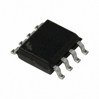
FIN1101MX Fairchild Semiconductor, FIN1101MX Datasheet - Page 2

FIN1101MX
Manufacturer Part Number
FIN1101MX
Description
IC REPEATER SGL PORT LVDS 8SOIC
Manufacturer
Fairchild Semiconductor
Type
Repeaterr
Datasheet
1.FIN1101MX.pdf
(6 pages)
Specifications of FIN1101MX
Tx/rx Type
LVDS
Delay Time
1.1ns
Capacitance - Input
2.2pF
Voltage - Supply
3 V ~ 3.6 V
Current - Supply
9.3mA
Mounting Type
Surface Mount
Package / Case
8-SOIC (3.9mm Width)
Supply Voltage (max)
3.6 V
Supply Voltage (min)
3 V
Maximum Operating Temperature
+ 150 C
Mounting Style
SMD/SMT
Interface
EIA/TIA-644-A
Minimum Operating Temperature
- 65 C
Supply Current
13.5 mA
Lead Free Status / RoHS Status
Lead free / RoHS Compliant
Available stocks
Company
Part Number
Manufacturer
Quantity
Price
www.fairchildsemi.com
V
V
V
V
V
V
I
I
I
I
I
I
V
C
C
Symbol
OS
IN
OFF
CCZ
CC
OZ
Absolute Maximum Ratings
DC Electrical Characteristics
Over supply voltage and operating temperature ranges, unless otherwise specified
Note 2: All typical values are at T
TH
TL
IH
IL
OD
V
OS
V
IC
Supply Voltage (V
LVDS DC Input Voltage (V
LVDS DC Output Voltage (V
Driver Short Circuit Current (I
Storage Temperature Range (T
Max Junction Temperature (T
Lead Temperature (T
ESD (Human Body Model)
ESD (Machine Model)
IN
OUT
OD
OS
(Soldering, 10 seconds)
Differential Input Threshold HIGH
Differential Input Threshold LOW
Input High Voltage (EN)
Input Low Voltage (EN)
Output Differential Voltage
V
Differential LOW-to-HIGH
Offset Voltage
Offset Magnitude Change from
Differential LOW-to-HIGH
Short Circuit Output Current
Input Current (EN, D
Power-Off Input or Output Current V
Disabled Power Supply Current
Power Supply Current
Disabled Output Leakage Current Driver Disabled, D
Common Mode Voltage Range
Input Capacitance
Output Capacitance
OD
Magnitude Change from
Parameter
CC
)
L
)
INX
A
IN
)
OUT
25 C and with V
, D
OSD
J
)
INX
STG
)
)
)
)
See Figure 1; V
See Figure 1; V
R
See Figure 2
D
V
V
Other Input
Drivers Disabled
Drivers Enabled, Any Valid Input Condition
D
|V
L
OUT
OD
IN
CC
OUT
ID
Continuous 10 mA
CC
|
100 , Driver Enabled,
0V to V
65 C to 150 C
0V, Driver Enabled
0V, V
100 mV to V
3.3V.
0.5V to 4.6V
0.5V to 4.6V
0.5V to 4.6V
(Note 1)
0V & D
0V to 3.6V
IN
CC
V
or V
CC
IC
IC
,
OUT
7000V
150 C
260 C
Test Conditions
OUT
300V
or 0V (for Differential Inputs)
OUT
CC
0.05V, 1.2V, or (V
0.05V, 1.2V, or (V
0V, Driver Enabled
0V to 3.6V
0V to 3.6V or
2
Supply Voltage (V
Operating Temperature (T
Magnitude of Input
Common Mode Input Voltage
Recommended Operating
Conditions
Note 1: The “Absolute Maximum Ratings”: are those values beyond which
damage to the device may occur. The databook specifications should be
met, without exception, to ensure that the system design is reliable over its
power supply, temperature and output/input loading variables. Fairchild
does not recommend operation of circuits outside databook specification.
Differential Voltage (|V
(V
IC
)
CC
CC
EN Input
Data Input
0.05V)
0.05V)
CC
)
0V
ID
1.125
GND
Min
250
2.0
100
A
|)
|V
)
ID|
/2
(0V
(Note 2)
1.23
Typ
330
3.2
9.3
2.2
2.0
2.6
3.4
3.4
|V
ID
|/2) to (V
V
CC
1.375
Max
V
13.5
100 mV to V
100
450
0.8
5.5
40 C to 85 C
25
25
(|V
CC
20
20
20
6
6
3.0V to 3.6V
CC
ID
|/2)
|V
Units
ID
mV
mV
mV
mV
mV
mA
mA
mA
mA
pF
pF
V
V
V
V
|/2)
A
A
A
CC


